Bit Addressable SFRs (alphabetical)
F-6
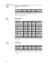
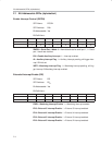
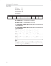
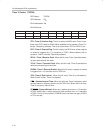
Port 3 (P3)
SFR Name: P3
SFR Address: B0
H
Bit−Addressable: Yes
Bit−Definitions:
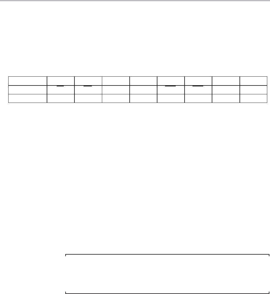
bit 7 bit 6 bit 5 bit 4 bit 3 bit 2 bit 1 bit 0
Name RD WR T1 T0 INT1 INT0 TXD RXD
Bit Address B7
H
B6
H
B5
H
B4
H
B3
H
B2
H
B1
H
B0
H
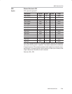
RD—Read Strobe. 0 = external memory read strobe.
WR—Write Strobe. 0 = external memory write strobe.
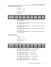
T1—Timer/Counter 1 External Input. Optionally used to control timer/counter
1 via external source.
T0—Timer/Counter 0 External Input. Optionally used to control timer/counter
0 via external source.
INT1—External Interrupt 1. Used to trigger external interrupt 1.
INT0—External Interrupt 0. Used to trigger external interrupt 0.
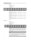
TXD—Serial Transmit Data. 8052 serial transmit line (from 8052 to external
device).
RXD—Serial Transmit Data. 8052 serial receive line (to 8052 from external
device).
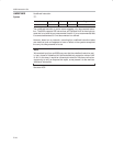
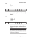
Note:
These bit names indicate the function of that I/O line on the P3 bus. A stan-
dard 8052 assembler will not recognize these bits by the given names; they
will only be recognized as P3.7, P3.6, etc.


