


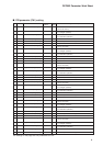
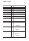
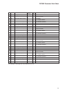
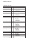
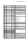
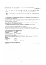
17
DCP552 Parameter Work Sheet
No. Item code Item
Factory default
User Settings and descriptions
settings
settings
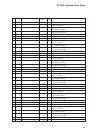
61 C 61 Programming system 0 0 : RAMP-X and RAMP-T (θ) combined
1:RAMP-X and RAMP-E (∆SP) combined
62 C 62 Program time unit 0 0 : Hours, min (SPU/hour for RAMP-T)
1:Min, sec (SPU/min for RAMP-T)
2:0.1 sec (SPU/sec for RAMP-T)
63 C 63
Time display (display panel 1
00:Remaining segment time
and 2)
1:total operation time (after READY → RUN start)
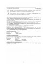
65 C 65
SP decimal point position (CH1)
10 to 4
66 C 66 SP limit lower limit PV1 range –19999 to +20000 SPU
lower limit
67 C 67 SP limit upper limit
PV1 range
–19999 to +20000 SPU
upper limit
68 C 68
SP decimal point position (CH2)
1 or 3 0 to 4 on a model without CP compensation.
0 to 3 on a model with CP compensation.
69 C 69 SP limit lower limit (CH2) PV2 range -19999 to +20000 SPU (CH2) on a model without CP
lower limit compensation.
0 to 2000 SPU(CH2) on a model with CP compensation.
70 C 70 SP limit upper limit (CH2)
PV2 range
upper limit
71 C 71 External switch input RSW5 0 0 : NOP (does not function)
1:RAMP-E
2:FAST
72 C 72 External switch input RSW6 0 3 : G.SOAK is cleared using OR
4:G.SOAK is cleared using AND
5:MANUAL/AUTO
73 C 73 External switch input RSW7 0 6 : AT start/terminate
7:NOP (does not function)
8:Auto load
74 C 74 External switch input RSW8 0 9 : NOP (does not function)
10 : NOP (does not function)
11 : O2 sensor check
75 C 75
External switch input RSW9 to 14
00:BCD4 bit + BCD2 bit
(program selection) 1: Binary 6 bits
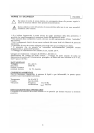
76 C 76 Communication address 0 0 to 127
77 C 77 Transmission rate 0 0 : 9600bps
1:4800bps
2:2400bps
3:1200bps
78 C 78 Transmission code 0 0 : 8 bits, even parity, 1 stop bit
1:8 bits, no parity, 2 stop bits
79 C 79 Communication protocol 0 0 : CPL
1:ST221 (no PV trend)
2:ST221 (PV trend)
80 C 80 Communication method 0 0 : RS-485
1:RS-232C
81 C 81 ROM ID — < Description >
82 C 82 ROM ITEM — Can only be referenced for mechanical service use.
83 C 83 ROM revision —
84 C 84 Data version —
85 C 85 CPU board ID —
86 C 86 I/O board ID —
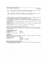
90 C 90 PID type 1 0 : Improved
1:Compatible with Mark I
91 C 91 PV1 burnout 0 0 : Provided
1:Not provided
92 C 92 PV2 burnout 0 0 : Provided
1:Not provided
93 C 93
Time proportional output system
00:Does not go on a second time in time proportional cycle.
(CH1) 1 : Goes on a second time in time proportional cycle.
94 C 94 Time proportional output 0 0 : Does not go on a second time in time proportional cycle
system (CH2) 1 : Goes on a second time in time proportional cycle