


Agilent E5250A User’s Guide, Edition 9 1-11
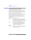
Introduction
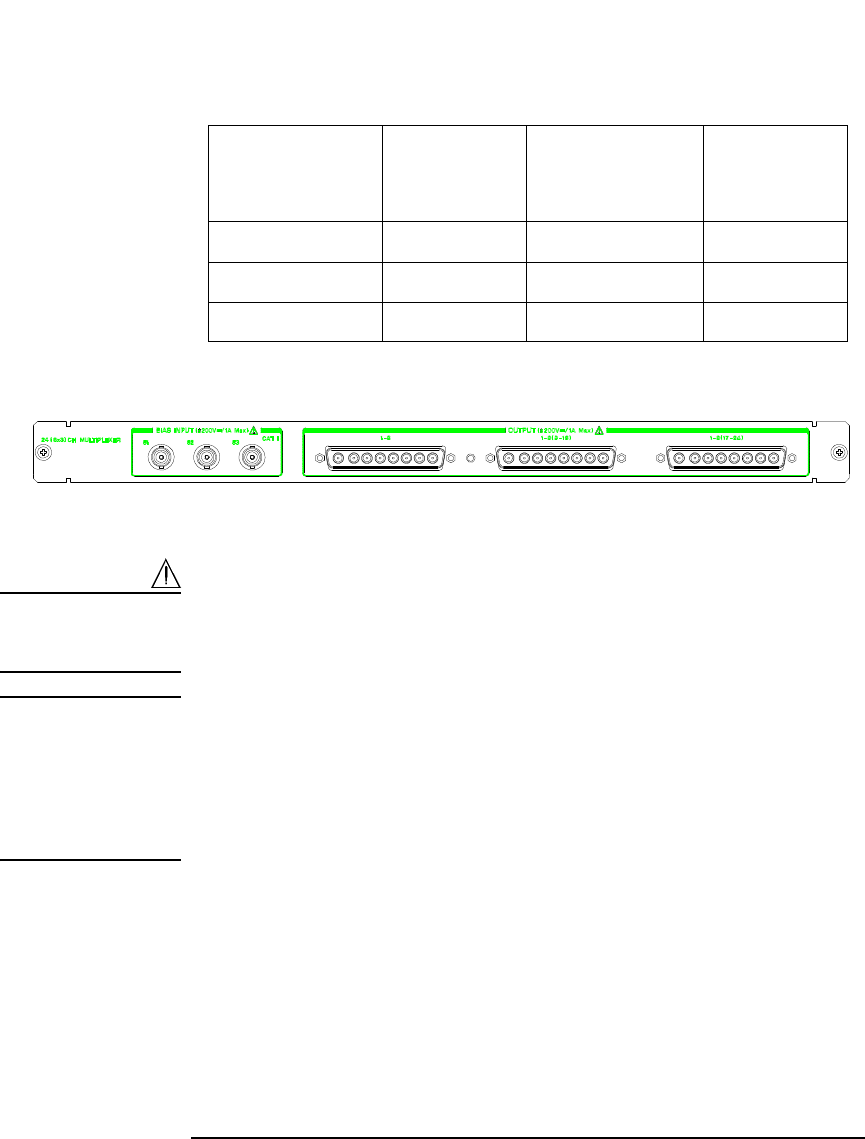
Agilent E5255A Product Description
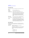
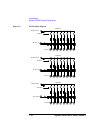
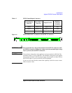
Table 1-2 E5255A Input/Output Connectors
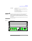
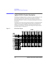
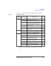
Figure 1-6 E5255A BIAS INPUT Connectors and OUTPUT Connectors
WARNING Do not touch the force and guard terminals of the OUTPUT connectors while
the E5250A is turned on. Dangerous voltages up to the maximum input voltage
may be present at the OUTPUT connectors.
CAUTION The maximum voltage that can be applied to any input terminal is ±200 Vdc. The
maximum current is 1 Adc at ±200 Vdc. The maximum voltage that can be applied
between input terminals is 300 Vdc. Do not apply an input signal over these limits to
the E5255A inputs. If you do, the E5255A will be damaged.
If you use a bias source that has current limit capability, set the bias source current
limit to less than 1 Adc.
2×8 multiplexer
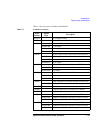
Block No.
BIAS INPUT
(Port No.)
Output Port No.
OUTPUT
Connector
(Location)
Block1 BIAS1 (51) Output 1 to 8 Left
Block2 BIAS2 (52) Output 9 to 16 Center
Block3 BIAS3 (53) Output 17 to 24 Right