


S1C88650 TECHNICAL MANUAL EPSON 103
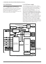
5 PERIPHERAL CIRCUITS AND THEIR OPERATION (Programmable Timer)
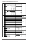
MODE16_A: 00FF30H•D7
MODE16_B: 00FF38H•D7
MODE16_C: 00FFB0H•D7
MODE16_D: 00FFB8H•D7
Selects either the 8/16 bit mode.
When "1" is written: 16 bits × 1 channel
When "0" is written: 8 bits × 2 channels
Reading: Valid
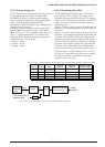
MODE16_A, MODE16_B, MODE16_C and
MODE16_D are the 8/16-bit mode selection
registers corresponding to Timers 0 and 1, Timers 2
and 3, Timers 4 and 5, and Timers 6 and 7,
respectively. Select whether Timer(L) and Timer(H)
are used as 2 channels independent 8-bit timers or
as 1 channel combined 16-bit timer.
When "0" is written to the MODE16_A (–D)
register, 8-bit × 2 channels is selected and when "1"
is written, 16-bit × 1 channel is selected.
At initial reset, this register is set to "0" (8-bit × 2
channels).
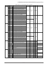
PTNREN_A: 00FF30H•D6
PTNREN_B: 00FF38H•D6
PTNREN_C: 00FFB0H•D6
PTNREN_D: 00FFB8H•D6
Enables/disables the noise rejecter in the external
clock input circuit.
When "1" is written: Enabled
When "0" is written: Disabled
Reading: Valid
Writing "1" to PTNREN_A (–D) enables the noise
rejecter for the external clock EXCL0 (–3). The noise
rejecter regards pulses less than a 16/fOSC1 seconds
in width as noise and rejects them.
When PTNREN_A (–D) is "0", the external clock
bypasses the noise rejecter.
At initial reset, this register is set to "0" (disabled).
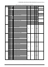
CKSEL0: 00FF30H•D0
CKSEL1: 00FF31H•D0
CKSEL2: 00FF38H•D0
CKSEL3: 00FF39H•D0
CKSEL4: 00FFB0H•D0
CKSEL5: 00FFB1H•D0
CKSEL6: 00FFB8H•D0
CKSEL7: 00FFB9H•D0
Selects the input clock for each timer.
When "1" is written: External clock
When "0" is written: Internal clock
Reading: Valid
The clock to be input to each timer is selected from
either the external clock (input signal of input
port) or the internal clock (prescaler output clock).
When "0" is written to the CKSELx register, the
internal clock (prescaler output INCLx) is selected
as the input clock for Timer x.
When "1" is written, the external clock (EXCL0
(K04 input) for Timers 0 and 1, EXCL1 (K05 input)
for Timers 2 and 3, EXCL2 (K06 input) for Timers 4
and 5, EXCL3 (K07 input) for Timers 6 and 7) is
selected and the timer functions as an event
counter.
In the 16-bit mode, the setting of the CKSEL(H)
register is invalid.
At initial reset, this register is set to "0" (internal
clock).
PRTF0: 00FF17H•D0
PRTF1: 00FF17H•D1
PRTF2: 00FF17H•D2
PRTF3: 00FF17H•D3
PRTF4: 00FF1BH•D0
PRTF5: 00FF1BH•D1
PRTF6: 00FF1BH•D2
PRTF7: 00FF1BH•D3
Selects the source clock for each timer (when
internal clock is used).
When "1" is written: fOSC1
When "0" is written: fOSC3
Reading: Valid
When "1" is written to the PRTFx register, the
OSC1 clock is selected as the source clock for
Timer x.
When "0" is written, the OSC3 clock is selected.
At initial reset, this register is set to "0" (f
OSC3).
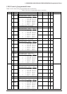
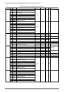
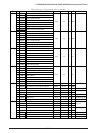
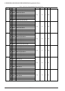
PST00–PST02: 00FF14H•D0–D2
PST10–PST12: 00FF14H•D4–D6
PST20–PST22: 00FF15H•D0–D2
PST30–PST32: 00FF15H•D4–D6
PST40–PST42: 00FF18H•D0–D2
PST50–PST52: 00FF18H•D4–D6
PST60–PST62: 00FF19H•D0–D2
PST70–PST72: 00FF19H•D4–D6
Selects the input clock for each timer (when internal
clock is used).
It can be selected from 8 types of division ratio
shown in Tables 5.10.9.1(a) and (b).
This register can also be read.
At initial reset, this register is set to "0".