


S1C88650 TECHNICAL MANUAL EPSON 89
5 PERIPHERAL CIRCUITS AND THEIR OPERATION (Programmable Timer)
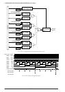
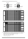
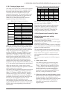
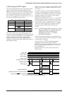
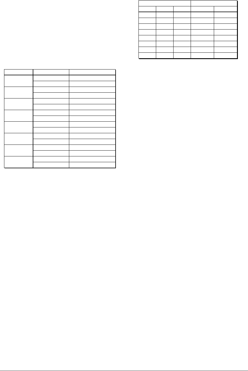
Table 5.10.3.2 Division ratio and control registers
(OSC1)
f
OSC1
/128
f
OSC1
/64
f
OSC1
/32
f
OSC1
/16
f
OSC1
/8
f
OSC1
/4
f
OSC1
/2
f
OSC1
/1
(OSC3)
f
OSC3
/4096
f
OSC3
/1024
f
OSC3
/256
f
OSC3
/64
f
OSC3
/32
f
OSC3
/8
f
OSC3
/2
f
OSC3
/1
PSTx2
1
1
1
1
0
0
0
0
Register Dividing ratio
PSTx1
1
1
0
0
1
1
0
0
PSTx0
1
0
1
0
1
0
1
0
The set clock is output to Timer x by writing "1" to
the clock control register PRPRTx.
When the 16-bit mode is selected, the program-
mable timer operates with the clock input to
Timer(L), and Timer(H) inputs the Timer(L)
underflow signal as the clock. Therefore, the
setting of Timer(H) input clock is invalid.
5.10.4 Operation and control of timer
Reload data register and setting
of initial value
The reload data register (RDRx) is used to set an
initial value of the down counter.
In the 8-bit mode, RDRx is used as an 8-bit register
separated for each timer.
In the 16-bit mode, the RDR(L) register is handled
as low-order 8 bits of reload data, and the RDR(H)
register is as high-order 8 bits.
The reload data register can be read and written,
and all the registers are set to FFH at initial reset.
Data written in this register is loaded into the
down counter, and a down counting starts from
the value.
The down counter is preset, in the following two
cases:
1) When software presets
The software preset can be done using the
preset control bits PSETx corresponding to
Timer x. When the preset control bit is set to
"1", the content of the reload data register is
loaded into the down counter at that point.
In the 16-bit mode, a 16-bit reload data is
loaded all at one time by setting PSET(L). In
this case, writing to PSET(H) is invalid.
2) When down counter has underflowed during a count
Since the down counter presets the reload data
by the underflow, the underflow period is
decided according to the value set in the reload
data register. This underflow generates an
interrupt, and controls the clock (TOUTx
signal) output.
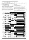
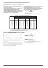
5.10.3 Setting of input clock
The clock to be input to the counter can be selected
from either the internal clock or external clock by
the input clock selection register (CKSEL) pro-
vided for each timer. The internal clock is an
output of the prescaler. The external clock is used
for the event counter function. A signal from the
input port is used as the count clock.
Table 5.10.3.1 shows the input clock selection
register and input clock of each timer.
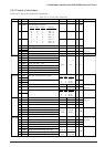
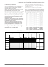
Table 5.10.3.1 Input clock selection
Timer
Timer 0
Timer 1
Timer 2
Timer 3
Timer 4
Timer 5
Timer 6
Timer 7
Register setting
CKSEL0 = "0"
CKSEL0 = "1"
CKSEL1 = "0"
CKSEL1 = "1"
CKSEL2 = "0"
CKSEL2 = "1"
CKSEL3 = "0"
CKSEL3 = "1"
CKSEL4 = "0"
CKSEL4 = "1"
CKSEL5 = "0"
CKSEL5 = "1"
CKSEL6 = "0"
CKSEL6 = "1"
CKSEL7 = "0"
CKSEL7 = "1"
Input clock
INCL0 (Prescaler)
EXCL0 (K04 input)
INCL1 (Prescaler)
EXCL0 (K04 input)
INCL2 (Prescaler)
EXCL1 (K05 input)
INCL3 (Prescaler)
EXCL1 (K05 input)
INCL4 (Prescaler)
EXCL2 (K06 input)
INCL5 (Prescaler)
EXCL2 (K06 input)
INCL6 (Prescaler)
EXCL3 (K07 input)
INCL7 (Prescaler)
EXCL3 (K07 input)
When the external clock is selected, a signal from
the input port is input to the programmable timer.
An noise rejecter is incorporated in the external
clock input circuit and it can be enabled/disabled
using the external clock noise rejecter select
registers PTNREN_A through PTNREN_D corre-
sponding to the EXCL0 through EXCL3 inputs.
Writing "1" to PTNREN_A (–D) enables the noise
rejecter for the external clock EXCL0 (–3). The
noise rejecter regards pulses less than a 16/fOSC1
seconds in width as noise and rejects them (an
external clock must have a pulse width at least
double the rejected width). When PTNREN_A (–D)
is "0", the external clock bypasses the noise rejecter.
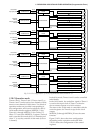
When the internal clock is used, select a source
clock and a division ratio of the prescaler to set the
clock frequency for each timer.
The source clock is specified using the source clock
selection register PRTFx provided for each timer.
When "1" is written to PRTFx, the OSC1 clock is
selected as the source clock for Timer x. When "0"
is written, the OSC3 clock is selected. The OSC3
oscillation circuit must be on before the OSC3 can
be used. See "5.4 Oscillation Circuits" for the
controlling of the OSC3 oscillation circuit.
The prescaler provides the division ratio selection
register PSTx0–PSTx2 for each timer. Note that the
division ratio varies depending on the selected
source clock.