S1C88650 TECHNICAL MANUAL EPSON 145
8 ELECTRICAL CHARACTERISTICS
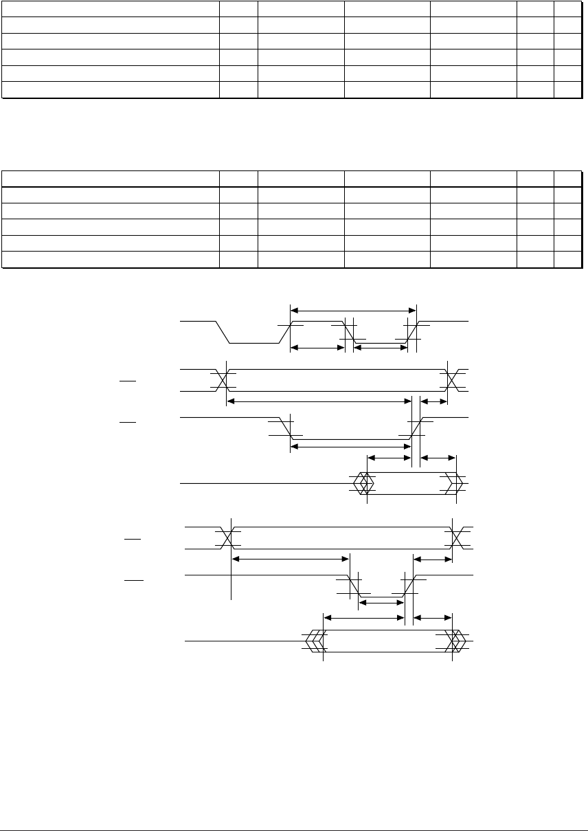
■ External memory access
• Read cycle
Item
Symbol
Min. Typ. Max. Unit
Address set-up time in read cycle
Address hold time in read cycle
Read signal pulse width
Data input set-up time in read cycle
Data input hold time in read cycle
t
ras
t
rah
t
rp
t
rds
t
rdh
ns
ns
ns
ns
ns
Note
1
1
Note) 1
Condition: V
DD
= 1.8 to 3.6 V, V
SS
= 0 V, Ta = 25°C, V
IH1
= 0.8V
DD
, V
IL1
= 0.2V
DD
, V
IH2
= 1.6 V, V
IL2
= 0.6 V,
V
OH
= 0.8V
DD
, V
OL
= 0.2V
DD
, C
L
= 100 pF (load capacitance)
Substitute the number of states for wait insertion in n.
t
c+
t
l-50+n•
t
c/2
t
h-40
t
c-10+n•
t
c/2
150
0
• Write cycle
Item
Symbol
Min. Typ. Max. Unit
Address set-up time in write cycle
Address hold time in write cycle
Write signal pulse width
Data output set-up time in write cycle
Data output hold time in write cycle
t
was
t
wah
t
wp
t
wds
t
wdh
ns
ns
ns
ns
ns
Note
1
1
Note) 1
Condition: V
DD
= 1.8 to 3.6 V, V
SS
= 0 V, Ta = 25°C, V
IH1
= 0.8V
DD
, V
IL1
= 0.2V
DD
, V
IH2
= 1.6 V, V
IL2
= 0.6 V,
V
OH
= 0.8V
DD
, V
OL
= 0.2V
DD
, C
L
= 100 pF (load capacitance)
Substitute the number of states for wait insertion in n.
t
c-90
t
h-40
t
l-20+n•
t
c/2
t
c-90+n•
t
c/2
t
h-40
t
h+40
ICLK
A00–A19
CE
RD
DIN
V
IH2
V
IL2
t
c
t
h
t
l
V
OH
V
OL
V
OH
V
OL
t
ras
t
rah
t
rdh
t
rds
V
IH1
V
IL1
t
rp
*
**
A00–A19
CE
WR
DOUT
V
OH
V
OL
V
OH
V
OL
t
was
t
wah
t
wdh
t
wds
V
IH1
V
IL1
t
wp
* In the case of crystal oscillation and ceramic oscillation:
t
h = 0.5
t
c ± 0.05
t
c,
t
l =
t
c -
t
h (1/
t
c: oscillation frequency)
* In the case of CR oscillation:
t
h = 0.5
t
c ± 0.10
t
c,
t
l =
t
c -
t
h (1/
t
c: oscillation frequency)


