S1C88650 TECHNICAL MANUAL EPSON 11
3 CPU AND BUS CONFIGURATION
3FFFFFH
:
100000H
0F0000H
0EFFFFH
010000H
00FFFFH
00D800H
00D7FFH
:
00C000H
00BFFFH
000000H
2FFFFFH
Internal memory
See Figure 3.2.1 for the internal memory
- MPU mode -
External
memory area
Internal memory
External
memory area
- MCU mode -
External
memory area
Internal memory
Unused area
Unused area
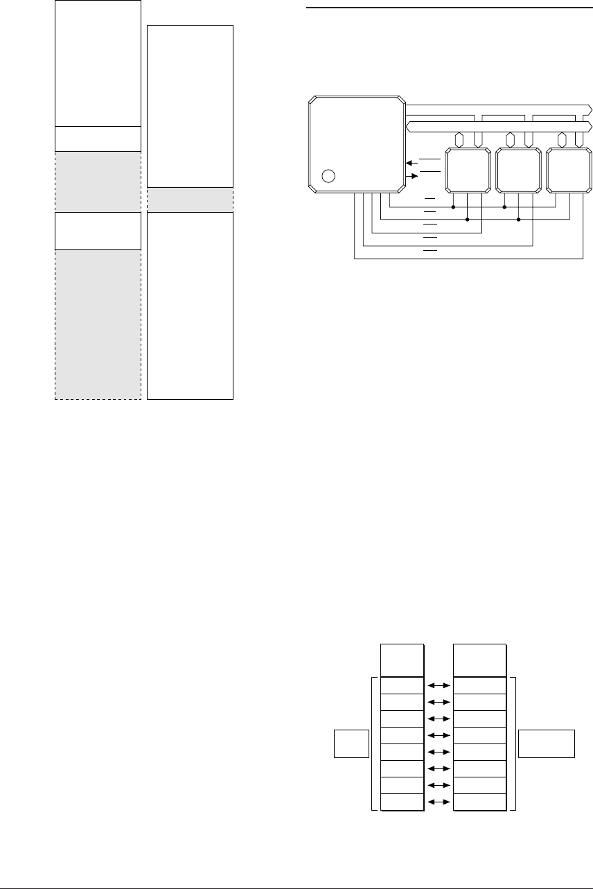
Fig. 3.5.2.2 Memory map for the expansion mode
There is an explanation on how all these settings
are actually made in "5.2 System Controller and Bus
Control" of this Manual.
3.5.3 CPU mode
The CPU allows software to select its operating
mode from two types shown below according to
the programming area size.
■ Minimum mode
The program area is configured within 64K
bytes in any one-bank. However, the bank to be
used must be specified in the CB register and
cannot be changed after an initialization. This
mode does not push the CB register contents
onto the stack when a subroutine is called. It
makes it possible to economize on stack area
usage. This mode is suitable for small- to mid-
scale program memory and large-scale data
memory systems.
■ Maximum mode
The program area can be configured exceeding
64K bytes. However the CB register must be
setup when the program exceeds a bank
boundary every 64K bytes. This mode pushes
the CB register contents when a subroutine is
called. This mode is suitable for large-scale
program and data memory systems.
3.6 External Bus
The S1C88650 has bus terminals that can address a
maximum of 1M × 3 bytes and memory (and other)
devices can be externally expanded according to
the range of each bus mode described in the
previous section.
S1C88650
External
device
Address bus (A0–A19)
Data bus (D0–D7)
RD
WR
CE0
CE1
CE2
BREQ
BACK
External
device
External
device
Fig. 3.6.1 External bus lines
Below is an explanation of external bus terminals.
For information on control methods, see Section 5.2,
"System Controller and Bus Control".
3.6.1 Data bus
The S1C88650 possesses an 8-bit external data bus
(D0–D7). The terminals and I/O circuits of data bus
D0–D7 are shared with I/O ports P00–P07, switch-
ing between these functions being determined by
the bus mode setting.
In the single chip mode, the 8-bit terminals are all
set as I/O ports P00–P07 and in the expansion
mode, they are set as data bus (D0–D7).
When set as data bus, the data register and I/O
control register of each I/O port are detached from
the I/O circuits and usable as a general purpose
data register with read/write capabilities.
The data bus can be pulled up to high during input
mode using the built-in pull-up resistor. This pull-
up resistor is enabled or disabled using the pull-up
control register and mask option. See "5.7 I/O
Ports" for details.
I/O
port
Data
bus
P00
P01
P02
P03
P04
P05
P06
P07
D0
D1
D2
D3
D4
D5
D6
D7
Bus modeBus mode
Single
chip
Expansion
Fig. 3.6.1.1 Correspondence between data bus
and I/O ports


