


S1C88650 TECHNICAL MANUAL EPSON 13
3 CPU AND BUS CONFIGURATION
_____ _____
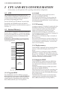
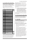
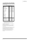
Table 3.6.4.1 CE0–CE2 address settings
CE0
CE1
CE2
300000H–3FFFFFH
100000H–1FFFFFH
200000H–2FFFFFH
000000H–00D7FFH, 010000H–0FFFFFH
100000H–1FFFFFH
200000H–2FFFFFH
Address range (expansion mode)
CE signal
MCU mode MPU mode
_____
When accessing the internal memory area, the CE
signal is not output. Care should be taken here
because the address range for these portions of
memory involves irregular settings.
The arrangement of memory space for external
devices does not necessarily have to be continuous
from a subordinate address and any of the chip
enable signals can be used to assign areas in
memory.
Note:
____
The CE signals will be inactive status when
the chip enters the standby mode (HALT
mode or SLEEP mode).
See Section 3.6.5, "WAIT control", for the output
timing of signal.
3.6.5 WAIT control
In order to insure accessing of external low speed
devices during high speed operations, the S1C88650
is equipped with a WAIT function which prolongs
access time. (See the "S1C88 Core CPU Manual" for
details of the WAIT function.)
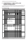
The WAIT state numbers to be inserted can be
selected in software from a series of 8 as shown in
Table 3.6.5.1.
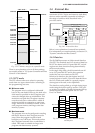
Table 3.6.5.1 Selectable WAIT state numbers
Selection No.
Insert states
1
0
2
2
3
4
4
6
5
8
6
10
7
12
8
14
* One state is a 1/2 cycle of the clock in length.
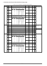
The WAIT states set in software are inserted
between bus cycle states T3–T4.
Note, however, that WAIT states cannot be inserted
when an internal register and internal memory are
being accessed and when operating with the OSC1
oscillation circuit (see "5.4 Oscillation Circuits").
Consequently, WAIT state settings are meaningless
in the single chip mode.
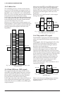
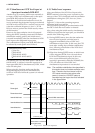
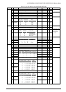
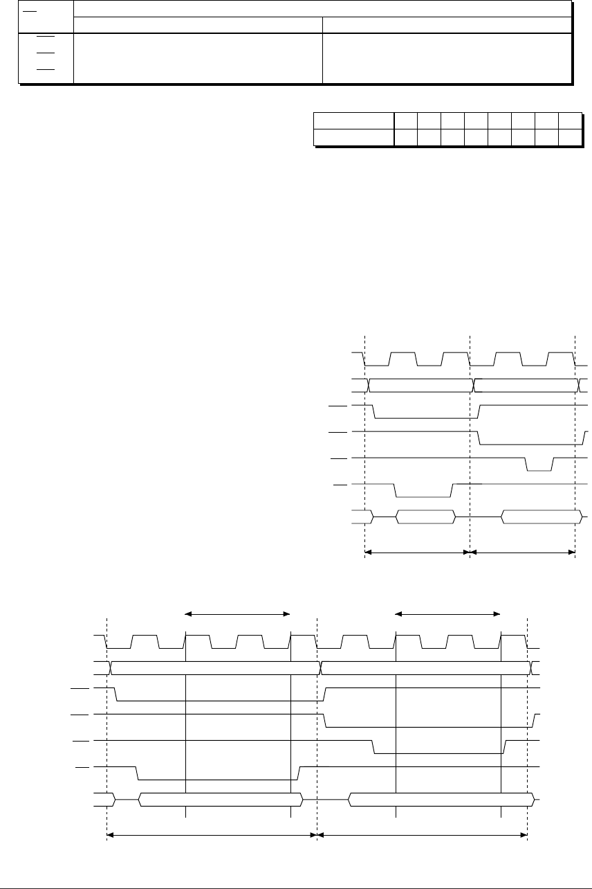
Figure 3.6.5.1 shows the memory read/write
timing charts.
CLK
A0–A19
CE0
CE1
WR
RD
D0–D7
T1
Read cycle
Address
T2 T3 T4
Read data
T1
Write cycle
Address
T2 T3 T4
Write data
(1) No WAIT
CLK
A0–A19
CE0
CE1
WR
RD
D0–D7
T1
Read cycle
Address
T2 T3 T4
Read data
T1
Write cycle
Address
T2 T3 T4
Write data
Tw2 Tw2Tw1 Tw1 Tw2 Tw2Tw1 Tw1
WAIT (4 states inserted) WAIT (4 states inserted)
(2) WAIT state insertion
Fig. 3.6.5.1 Memory read/write cycle