


70 EPSON S1C88650 TECHNICAL MANUAL
5 PERIPHERAL CIRCUITS AND THEIR OPERATION (Serial Interface)
(6) Clock source control
When the programmable timer is selected for
the clock source, set transfer rate on the pro-
grammable timer side. (See "5.10 Programmable
Timer".)
When the divided signal of OSC3 oscillation
circuit is selected for the clock source, be sure
that the OSC3 oscillation circuit is turned ON
prior to commencing data transfer. (See "5.4
Oscillation Circuits".)
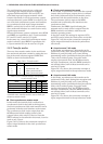
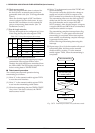
(7) Stop bit length selection
The stop bit length can be configured to 1 bit or
2 bits using the stop bit select register STPB.
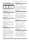
Table 5.8.7.1 Stop bit and parity bit settings
EPR
1
0
1
0
STPB
1
0
PMD
1
0
–
1
0
–
Stop bit
2 bits
2 bits
2 bits
1 bit
1 bit
1 bit
Parity bit
Odd
Even
Non parity
Odd
Even
Non parity
Settings
(8) Serial data input/output permutation
The S1C88650 provides the data input/output
permutation select register SDP to select
whether the serial data bits are transfered from
the LSB or MSB. The SDP register should be set
before writing data to TRXD0–TRXD7.
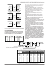
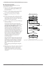
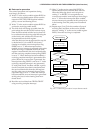
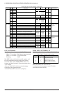
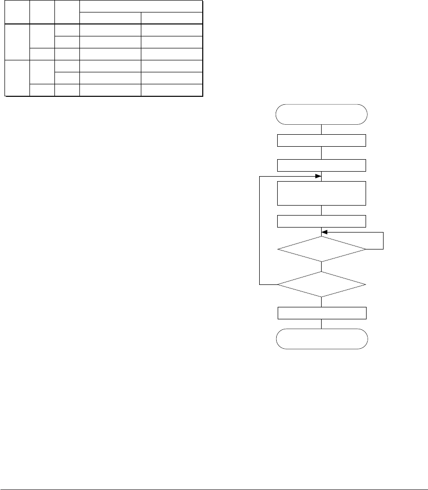
■ Data transmit procedure
The control procedure and operation during
transmitting is as follows.
(1) Write "0" in the transmit enable register TXEN
to reset the serial interface.
(2) Write "1" in the transmit enable register TXEN
to set into the transmitting enable status.
(3)
Write the transmitting data into TRXD0–TRXD7.
Also, when 7-bit data is selected, the TRXD7
data becomes invalid.
Data transmitting
End
TXEN ← 0
No
Yes
Transmit complete ?
Set transmitting data
to TRXD0–TRXD7
No
Yes
FSTRA = 1 ?
TXEN ← 0
TXTRG ← 1
TXEN ← 1
Fig. 5.8.7.2 Transmit procedure in asynchronous mode
(4) Write "1" in the transmit control bit TXTRG and
start transmitting.
This control causes the shift clock to change to
enable and a start bit (LOW) is output to the
SOUT terminal in synchronize to its rising edge.
The transmitting data set to the shift register is
shifted one bit at a time at each rising edge of
the clock thereafter and is output from the
SOUT terminal. After the data output, it outputs
a stop bit (HIGH) and HIGH level is maintained
until the next start bit is output.
The transmitting complete interrupt factor flag
FSTRA is set to "1" at the point where the data
transmitting is completed. When interrupt has
been enabled, a transmitting complete interrupt
is generated at this point.
Set the following transmitting data using this
interrupt.
(5) Repeat steps (3) to (4) for the number of bytes of
transmitting data, and then set the transmit
disable status by writing "0" to the transmit
enable register TXEN, when the transmitting is
completed.