86 EPSON S1C88650 TECHNICAL MANUAL
5 PERIPHERAL CIRCUITS AND THEIR OPERATION (Programmable Timer)
5.10 Programmable Timer
5.10.1 Configuration of
programmable timer
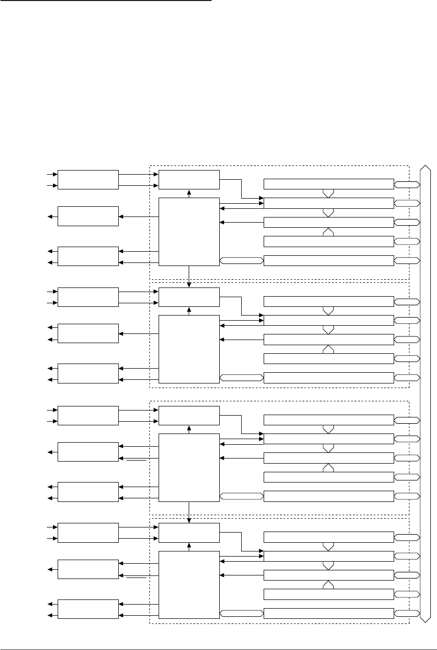
The S1C88650 has four built-in 16-bit program-
mable timer systems. Each system timer consists of
a 16-bit presettable down counter, and can be used
as 16-bit × 1 channel or 8-bit × 2 channels of
programmable timer. Furthermore, they function
as event counters using the input port terminal.
Figures 5.10.1.1 and 5.10.1.2 shows the configura-
tion of the 16-bit programmable timers.
Two 8-bit down counters, the reload data register
and compare data register corresponding to each
down counter are arranged in the 16-bit program-
mable timer.
The reload data register is used to set an initial
value to the down counter.
The compare data register stores data for
comparison with the content of the down counter.
By setting these registers, a PWM waveform is
generated and it can be output to external devices
as the TOUT0, 1, 2 or 3 signal. Furthermore, the
serial interface clock is generated from the Timer 1
underflow signal. The Timer 5 underflow signal can
be used to set the frame frequency for the LCD
driver.
Data bus
8-bit reload data register (RDR0)
8-bit down counter (PTM0)
8-bit compare data register (CDR0)
Timer 0 control registers
Control circuit
Clock selection
circuit
Prescaler/clock
control circuit
Clock output circuit
Comparator
Underflow
Underflow signal
INCL0
fOSC3/fOSC1
Input port (K04)
Clock output
EXCL0
TOUT0
Underflow
interrupt
Compare match
interrupt
Compare match
Timer 0
Interrupt circuit
8-bit reload data register (RDR1)
8-bit down counter (PTM1)
8-bit compare data register (CDR1)
Timer 1 control registers
Control circuit
Clock selection
circuit
Prescaler/clock
control circuit
Clock output circuit
Comparator
Underflow
INCL1
fOSC3/fOSC1
Input port (K04)
Clock output
EXCL0
TOUT1
Underflow
interrupt
Compare match
interrupt
To serial I/F
Compare match
Timer 1
Interrupt circuit
8-bit reload data register (RDR2)
8-bit down counter (PTM2)
8-bit compare data register (CDR2)
Timer 2 control registers
Control circuit
Clock selection
circuit
Prescaler/clock
control circuit
Clock output circuit
Comparator
Underflow
Underflow signal
INCL2
fOSC3/fOSC1
Input port (K05)
Clock output
EXCL1
TOUT2
Underflow
interrupt
Compare match
interrupt
Compare match
Timer 2
Interrupt circuit
8-bit reload data register (RDR3)
8-bit down counter (PTM3)
8-bit compare data register (CDR3)
Timer 3 control registers
Control circuit
Clock selection
circuit
Prescaler/clock
control circuit
Clock output circuit
Comparator
Underflow
INCL3
fOSC3/fOSC1
Input port (K05)
Clock output
EXCL1
TOUT3
TOUT2
TOUT3
Underflow
interrupt
Compare match
interrupt
Compare match
Timer 3
Interrupt circuit
Fig. 5.10.1.1 Configuration of 16-bit programmable timer (Timers 1–3)


