


122 EPSON S1C88650 TECHNICAL MANUAL
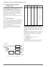
5 PERIPHERAL CIRCUITS AND THEIR OPERATION (LCD Driver)
DTFNT: 00FF10H•D2
Selects the dot font.
When "1" is written: 12 × 12 dots
When "0" is written: 16 × 16/5 × 8 dots
Reading: Valid
Select 16 × 16/5 × 8 dots or 12 × 12 dots type for the
display memory area.
When "0" is written to DTFNT, 16 × 16/5 × 8 dots is
selected and when "1" is written, 12 × 12 dots is
selected.
The correspondence between the display memory
bits set according to the dot font, and the common/
segment terminals are shown in Figures 5.11.5.1–
5.11.5.5.
At initial reset, DTFNT is set to "0" (16 × 16/5 × 8
dots).
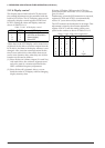
SEGREV: 00FF10H•D6
Reverses the memory allocation for the SEG
terminals.
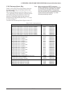
Table 5.11.7.3 Selecting SEG assignment
SEGREV
1
0
Assignment
Reverse
Normal
Fx00H
SEG125
SEG0
Fx70H
SEG0
SEG125
At initial reset, SEGREV is set to "0" (normal).
DSPAR: 00FF11H•D6
Selects the display area.
When "1" is written: Display area 1
When "0" is written: Display area 0
Reading: Valid
An area to be displayed is selected from two areas
in the display memory.
When "0" is written to DSPAR, display area 0 is
selected and when "1" is written, display area 1 is
selected.
The correspondence between the display memory
bits set according to the display area, and the
common/segment terminals are shown in Figures
5.11.5.1–5.11.5.5.
At initial reset, DSPAR is set to "0" (display area 0).
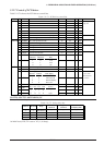
LCDC0, LCDC1: 00FF11H•D4, D5
Controls the LCD display.
Table 5.11.7.4 LCD display control
LCDC1 LCDC0 LCD display
1
1
0
0
1
0
1
0
All LCDs lit (Static)
All LCDs out (Dynamic)
Normal display
Drive OFF
The four settings mentioned above can be made
without changing the display memory data.
At initial reset and in the SLEEP status, this register
is set to "0" (drive off).
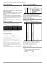
LC0–LC3: 00FF11H•D0–D3
Adjusts the LCD contrast.
Table 5.11.7.5 LCD contract adjustment
LC3 LC0 Contrast
1
1
1
1
1
1
1
1
0
0
0
0
0
0
0
0
1
0
1
0
1
0
1
0
1
0
1
0
1
0
1
0
Dark
↑
↓
Light
LC1
1
1
0
0
1
1
0
0
1
1
0
0
1
1
0
0
LC2
1
1
1
1
0
0
0
0
1
1
1
1
0
0
0
0
The contrast can be adjusted in 16 stages as
mentioned above. This adjustment changes the
drive voltage on terminals VC1 to VC5.
At initial reset, this register is set to "0".
FRMCS: 00FF11H•D7
Selects the source clock for generating the frame
signal.
When "1" is written: Programmable timer 5
When "0" is written: fOSC1
Reading: Valid
When "0" is written to FRMCS, f
OSC1 is selected,
and when "1" is written, programmable timer 5 is
selected.
At initial reset, FRMCS is set to "0" (fOSC1).