


S1C88650 TECHNICAL MANUAL EPSON i
CONTENTS
Contents
1 INTRODUCTION .............................................................................................. 1
1.1 Features .............................................................................................................................1
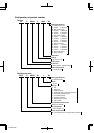
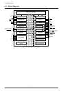
1.2 Block Diagram ...................................................................................................................2
1.3 Pins ....................................................................................................................................3
1.3.1 Pin layout diagram ................................................................................................................... 3
1.3.2 Pin description .........................................................................................................................4
1.4 Mask Option.......................................................................................................................5
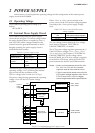
2 POWER SUPPLY............................................................................................... 7
2.1 Operating Voltage..............................................................................................................7
2.2 Internal Power Supply Circuit ...........................................................................................7
3 CPU AND BUS CONFIGURATION ................................................................ 8
3.1 CPU ...................................................................................................................................8
3.2 Internal Memory ................................................................................................................8
3.2.1 Program ROM ..........................................................................................................................8
3.2.2 RAM..........................................................................................................................................8
3.2.3 I/O memory............................................................................................................................... 8
3.2.4 Display memory........................................................................................................................ 8
3.2.5 Kanji font ROM ........................................................................................................................ 8
3.3 Exception Processing Vectors ...........................................................................................9
3.4 CC (Customized Condition Flag) ......................................................................................9
3.5 Chip Mode..........................................................................................................................9
3.5.1 MCU mode and MPU mode .....................................................................................................9
3.5.2 Bus mode .................................................................................................................................10
3.5.3 CPU mode ............................................................................................................................... 11
3.6 External Bus......................................................................................................................11
3.6.1 Data bus ..................................................................................................................................11
3.6.2 Address bus ............................................................................................................................. 12
3.6.3 Read (RD)/write (WR) signals.................................................................................................12
3.6.4 Chip enable (CE) signal .......................................................................................................... 12
3.6.5 WAIT control ...........................................................................................................................13
3.6.6 Bus authority release state ...................................................................................................... 14
4 INITIAL RESET ............................................................................................... 15
4.1 Initial Reset Factors..........................................................................................................15
4.1.1 RESET terminal .......................................................................................................................15
4.1.2 Simultaneous LOW level input at input port terminals K00–K03........................................... 16
4.1.3 Initial reset sequence ............................................................................................................... 16
4.2 Initial Settings After Initial Reset......................................................................................17
5 PERIPHERAL CIRCUITS AND THEIR OPERATION................................ 18
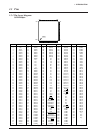
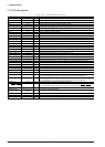
5.1 I/O Memory Map ..............................................................................................................18
5.2 System Controller and Bus Control ..................................................................................34
5.2.1 Bus mode and CPU mode settings ..........................................................................................34
5.2.2 Address decoder (CE output) settings ..................................................................................... 34
5.2.3 WAIT state settings ..................................................................................................................35
5.2.4 Setting the bus authority release request signal...................................................................... 35
5.2.5 Stack page setting ....................................................................................................................35
5.2.6 Control of system controller....................................................................................................36
5.2.7 Programming notes .................................................................................................................38