


S1C88650 TECHNICAL MANUAL EPSON 165
APPENDIX A S5U1C88000P1&S5U1C88649P2 MANUAL (Peripheral Circuit Board for S1C88650)
(21) LED 13 (Reserved)
Unused.
(22) LED 14 (OSC1 operating clock)
The OSC1 operating clock is connected to this
LED. The corresponding monitor pin (pin 14)
can be used to check the OSC1 clock frequency.
(23) LED 15 (OSC3 operating clock)
The OSC3 operating clock is connected to this
LED. The corresponding monitor pin (pin 15)
can be used to check the OSC3 clock frequency.
(24) LED 16 (FPGA configuration)
If the FPGA on the S5U1C88000P1 includes
circuit data, this LED lights when the power is
turned on. If this LED does not light at power-
up, a circuit data must be written to the FPGA
before debugging can be started (turn the
power on again after writing data).
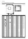
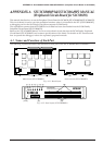
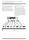
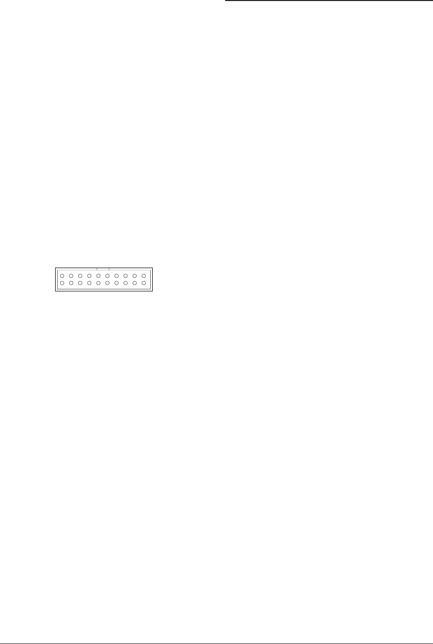
(25) LED signal monitor connector
This connector provides the signals that drive the
LEDs shown above for monitoring. The signals
listed below are output from the connector pins.
The signal level is high when the LED is lit and is
low when the LED is not lit.
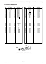
2468101214161820
135791113151719
Fig. A.1.3 LED signal monitor connector
Pin 1: LED 1 (MPU/MCU mode)
Pin 2: LED 2 (Bus mode 1)
Pin 3: LED 3 (CPU mode 0)
Pin 4: LED 4 (CPU operating clock)
Pin 5: LED 5 (OSC3 oscillation status)
Pin 6: LED 6 (SVD circuit status)
Pin 7: LED 7 (LCD circuit status)
Pin 8: LED 8 (Heavy load protection status)
Pin 9: LED 9 (HALT/SLEEP, RUN status)
Pin 10: LED 10 (
LCD voltage regulator power status
)
Pin 11: LED 11 (Power voltage booster status)
Pin 12: LED 12 (SEG output assignment status)
Pin 14: OSC1 operating clock
Pin 15: OSC3 operating clock
Pin 18: OSC1 CR oscillation frequency monitor pin
Pin 19: OSC3 CR oscillation frequency monitor pin
Pins 13 , 17 and 20 are not used.
The OSC3 CR oscillation clock is connected to
pins 18 and 19. (The CR oscillation circuit on
this board always operates even if crystal
oscillation is selected by mask option and
regardless of the SOSC3 register status.) These
pins can be used to monitor CR oscillation
when adjusting the oscillation frequency.
(26) I/O #1, I/O #2, I/O #3, I/O #4 connectors
These are the connectors for connecting the I/
O and LCD. The I/O cables (80-pin/40-pin × 2
flat type, 100-pin/50-pin × 2 flat type, 40-pin/
20-pin × 2 flat type) are used to connect to the
target system.
A.2 Precautions
Take the following precautions when using the
S5U1C88000P1&S5U1C88649P2.
A.2.1 Precaution for operation
(1) Turn the power of all equipment off before
connecting or disconnecting cables.
(2) Make sure that the input ports (K00–K03) are
not all set to low when turning the power on
until the mask option data is loaded, as the
key-entry reset function may activated.
(3) The mask option data must be loaded before
debugging can be started.
A.2.2 Differences from actual IC
Caution is called for due to the following function
and property related differences with the actual
IC. If these precautions are overlooked, it may not
operate on the actual IC, even if it operates on the
ICE in which the S5U1C88000P1&S5U1C88649P2
has been installed.
(1) I/O differences
Interface power voltage
This board and target system interface voltage
is set to +3.3 V. To obtain the same interface
voltage as in the actual IC, attach a level shifter
or similar circuit on the target system side to
accommodate the required interface voltage.
Drive capability of each output port
The drive capability of each output port on this
board is higher than that of the actual IC.
When designing the application system and
software, refer to Chapter 8, "ELECTRICAL
CHARACTERISTICS" to confirm the drive
capability of each output port.
Input port characteristics
The AC characteristic of the input terminal is
different from that of the actual IC and it
affects the input interrupt function. Therefore,
evaluate the operation in the actual IC if the
rise/fall time of the input signal is long.
Protective diode of each port
All I/O ports incorporate a protective diode
for VDD and VSS, and the interface signals
between this board and the target system are
set to +3.3 V. Therefore, this board and the
target system cannot be interfaced with a
voltage exceeding VDD even if the output ports
are configured with open-drain output.