


S1C88650 TECHNICAL MANUAL EPSON 29
5 PERIPHERAL CIRCUITS AND THEIR OPERATION (I/O Memory Map)
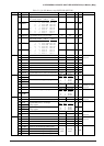
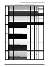
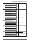
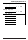
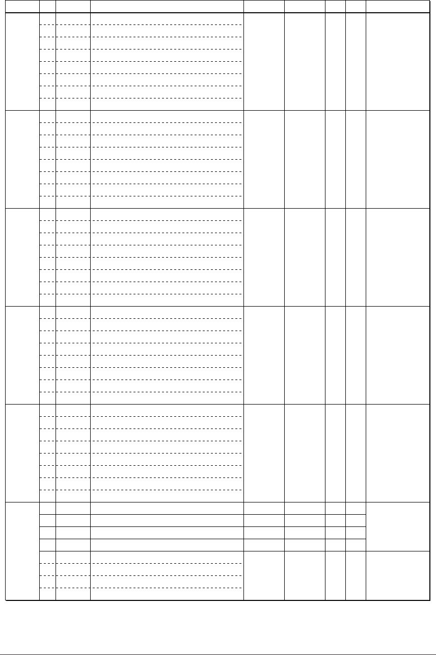
Table 5.1.1(l) I/O Memory map (00FF61H–00FF70H)
SR R/WAddress Bit Name Function Comment10
00FF61 D7
D6
D5
D4
D3
D2
D1
D0
IOC17
IOC16
IOC15
IOC14
IOC13
IOC12
IOC11
IOC10
0 R/W
Output Input
P17 I/O control register
P16 I/O control register
P15 I/O control register
P14 I/O control register
P13 I/O control register
P12 I/O control register
P11 I/O control register
P10 I/O control register
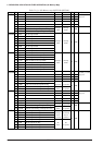
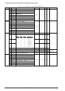
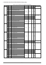
00FF62 D7
D6
D5
D4
D3
D2
D1
D0
P07D
P06D
P05D
P04D
P03D
P02D
P01D
P00D
P07 I/O port data
P06 I/O port data
P05 I/O port data
P04 I/O port data
P03 I/O port data
P02 I/O port data
P01 I/O port data
P00 I/O port data
1 R/W
High Low
00FF63 D7
D6
D5
D4
D3
D2
D1
D0
P17D
P16D
P15D
P14D
P13D
P12D
P11D
P10D
1 R/W
High Low
P17 I/O port data
P16 I/O port data
P15 I/O port data
P14 I/O port data
P13 I/O port data
P12 I/O port data
P11 I/O port data
P10 I/O port data
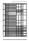
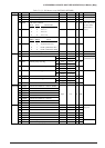
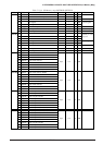
00FF64 D7
D6
D5
D4
D3
D2
D1
D0
PULP07
PULP06
PULP05
PULP04
PULP03
PULP02
PULP01
PULP00
1 R/W
On Off
P07 pull-up control register
P06 pull-up control register
P05 pull-up control register
P04 pull-up control register
P03 pull-up control register
P02 pull-up control register
P01 pull-up control register
P00 pull-up control register
00FF65 D7
D6
D5
D4
D3
D2
D1
D0
PULP17
PULP16
PULP15
PULP14
PULP13
PULP12
PULP11
PULP10
1 R/W
On Off
P17 pull-up control register
P16 pull-up control register
P15 pull-up control register
P14 pull-up control register
P13 pull-up control register
P12 pull-up control register
P11 pull-up control register
P10 pull-up control register
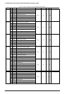
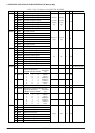
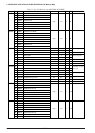
00FF70 D7
D6
D5
D4
D3
D2
D1
D0
–
–
–
–
HZR1H
HZR1L
HZR0H
HZR0L
R/W register
R/W register
R/W register
R/W register
R14–R17 high impedance control
R10–R13 high impedance control
R04–R07 high impedance control
R00–R03 high impedance control
Reserved register
0
0
0
0
0
R/W
R/W
R/W
R/W
R/W
1
1
1
1
High
impedance
0
0
0
0
Comple-
mentary