Vol. 2A 2-5
INSTRUCTION FORMAT
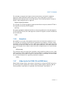
location; the last eight (Mod = 11B) provide ways of specifying general-purpose,
MMX technology and XMM registers.
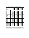
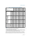
The Mod and R/M columns in Table 2-1 and Table 2-2 give the binary encodings of the
Mod and R/M fields required to obtain the effective address listed in the first column.
For example: see the row indicated by Mod = 11B, R/M = 000B. The row identifies
the general-purpose registers EAX, AX or AL; MMX technology register MM0; or XMM
register XMM0. The register used is determined by the opcode byte and the operand-
size attribute.
Now look at the seventh row in either table (labeled “REG =”). This row specifies the
use of the 3-bit Reg/Opcode field when the field is used to give the location of a
second operand. The second operand must be a general-purpose, MMX technology,
or XMM register. Rows one through five list the registers that may correspond to the
value in the table. Again, the register used is determined by the opcode byte along
with the operand-size attribute.
If the instruction does not require a second operand, then the Reg/Opcode field may
be used as an opcode extension. This use is represented by the sixth row in the
tables (labeled “/digit (Opcode)”). Note that values in row six are represented in
decimal form.
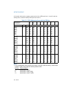
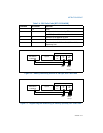
The body of Table 2-1 and Table 2-2 (under the label “Value of ModR/M Byte (in Hexa-
decimal)”) contains a 32 by 8 array that presents all of 256 values of the ModR/M
byte (in hexadecimal). Bits 3, 4 and 5 are specified by the column of the table in
which a byte resides. The row specifies bits 0, 1 and 2; and bits 6 and 7. The figure
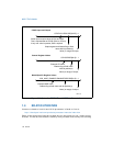
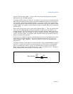
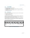
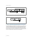
below demonstrates interpretation of one table value.
Figure 2-2. Table Interpretation of ModR/M Byte (C8H)
Mod 11
RM 000
REG = 001
C8H 11001000
/digit (Opcode);


