Vol. 2A 3-421
INSTRUCTION SET REFERENCE, A-M
FXSAVE—Save x87 FPU, MMX Technology, SSE, and SSE2 State
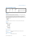
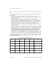
The FXSAVE instruction saves an abridged version of the x87 FPU tag word in the
FTW field (unlike the FSAVE instruction, which saves the complete tag word). The tag
information is saved in physical register order (R0 through R7), rather than in top-of-
stack (TOS) order. With the FXSAVE instruction, however, only a single bit (1 for valid
or 0 for empty) is saved for each tag. For example, assume that the tag word is
currently set as follows:
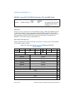
R7 R6 R5 R4 R3 R2 R1 R0
11 xx xx xx 11 11 11 11
Here, 11B indicates empty stack elements and “xx” indicates valid (00B), zero (01B),
or special (10B).
For this example, the FXSAVE instruction saves only the following 8 bits of informa-
tion:
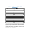
R7 R6 R5 R4 R3 R2 R1 R0
01110000
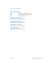
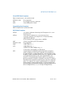
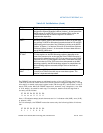
MXCSR MXCSR Register State (32 bits). See Figure 10-3 in the Intel® 64 and IA-32
Architectures Software Developer’s Manual, Volume 1, for the layout of the
MXCSR register. If the OSFXSR bit in control register CR4 is not set, the
FXSAVE instruction may not save this register. This behavior is
implementation dependent.
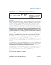
MXCSR_
MASK
MXCSR_MASK (32 bits). This mask can be used to adjust values written to
the MXCSR register, ensuring that reserved bits are set to 0. Set the mask
bits and flags in MXCSR to the mode of operation desired for SSE and SSE2
SIMD floating-point instructions. See “Guidelines for Writing to the MXCSR
Register” in Chapter 11 of the Intel® 64 and IA-32 Architectures Software
Developer’s Manual, Volume 1, for instructions for how to determine and
use the MXCSR_MASK value.
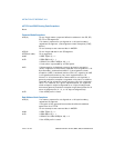
ST0/MM0 through
ST7/MM7
x87 FPU or MMX technology registers. These 80-bit fields contain the x87
FPU data registers or the MMX technology registers, depending on the
state of the processor prior to the execution of the FXSAVE instruction. If
the processor had been executing x87 FPU instruction prior to the FXSAVE
instruction, the x87 FPU data registers are saved; if it had been executing
MMX instructions (or SSE or SSE2 instructions that operated on the MMX
technology registers), the MMX technology registers are saved. When the
MMX technology registers are saved, the high 16 bits of the field are
reserved.
XMM0 through
XMM7
XMM registers (128 bits per field). If the OSFXSR bit in control register CR4
is not set, the FXSAVE instruction may not save these registers. This
behavior is implementation dependent.
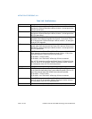
Table 3-49. Field Definitions (Contd.)
Field Definition


