


DFX-8500
Rev. B
1-20
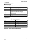
Signal Level: TTL-level compatible, IEEE-1284 level 1 device
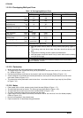
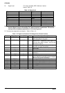
Refer to Table 1-9.
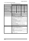
Table 1-9. Signal Level
Parameter Minimum Maximum Condition
VOH* - 5.5 V
VOL* -0.5 V -
IOH* - 0.32 mA VOH = 2.4 V
IOL* - 12 mA VOL = 0.4 V
CO - 50 pF
VIH - 2.0 V
VIL 0.8 V -
IIH - 0.32 mA VIH = 2.4 V
IIL - 12 mA VIL = 0.8 V
CI - 50 pF
Note: * A low logic level on the logical high signal is 2.0 V or less when the printer is powered off.
And this signal is equal or exceeding 3. 0 V when the printer is powered on. The receiver
shall provide an impedance equivalent to 7.5 K ohms to ground.
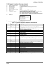
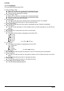
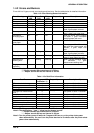
Connector pin assignments and signals: Refer to Table 1-10.
Table 1-10. Signal and Connector Pin Assignment (Forward channel)
Pin No. Signal Name Return GND pin In/Out* Functional Description
1 /STROBE 19 In The strobe pulse. Read-in of data is performed
at the falling edge of this pulse.
2-9 DATA 0-7 20-27 In The DATA0 through DATA7 signals represent
data bits 0 to 7, respectively. Each signal is at
high level when data is logical 1 and low level
when data is logical 0.
10 /ACKNLG 28 Out This signal is a negative pulse indicating that
the printer can again accept data.
11 BUSY 29 Out A high signal indicates that the printer cannot
receive data.
12 PE 28 Out A high signal indicates paper-out error.
13 SLCT 28 Out Always at high level when the printer is
powered on.
14 /AFXT 30 In Not used.
31 /INIT 30 In The falling edge of a negative pulse or a low
signal on this line causes the printer to initialize.
Minimum 50 us pulse is necessary.
32 /ERROR 29 Out A low signal indicates printer error condition.
36 /SLIN 30 In Not used.
18 Logic H - Out Pulled up to +5V via 3.9K ohm resistor.
35 +5V - Out Pulled up to +5V via 3.3K ohm resistor.
17 Chassis GND - - Chassis GND.
16,33,19,30 GND - - Signal GND.
15,34 NC - - Not connected.
Note: * In/Out refers to the direction of signal flow from the printer’s point of view.