


OPERATING PRINCIPLES
Rev. B
2-3
3
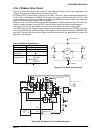
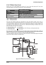
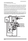
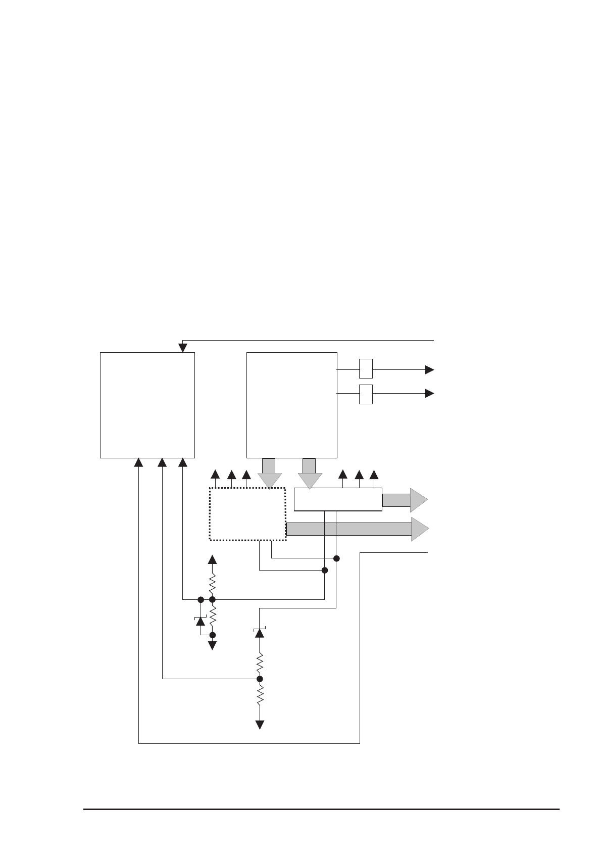
2.3.9 Printhead Drive Circuit
Figure 2-27 shows a printhead drive circuit block diagram.
General :
The print data lines from IC1 are active when they are HIGH. When ports HDR1 (HDL1) to HDR9 (HDL9)
of IC1 go HIGH, the FET gates are biased, and the FETs are turned on to apply the current to the
printhead coil. At the same time, ports HDRS1 (HDLS1) to HDRS9 (HDLS9) of IC1 go HIGH, the FET
gates are biased, and the FETs are turned on because the each printhead coil is driven by bipolar drive
method. When the HD port of IC1 goes LOW, the FET is turned off and the printhead coil current is cut.
Two +37 VDC lines (VP1-GP1 on the C204 DRV-B board and VP2-GP2 on the C204 MAIN board) assign
the common voltage for the printhead coil. Pins #1, #2, #7, #9, #10, #11, #12, #16, and #17 are supplied
by the VP2-GP2 line (CN1 on the C204 MAIN board). Pins #3, #4, #5, #6 #8, #13, #14, #15, and #18 are
supplied by the VP1-GP1 line (CN1 on the C204 DRV-B board).
The CPU monitors the printhead temperature and head fan (HF) temperature. When the temperature
rises abnormally, printing stops at once until the temperature cools.
The CPU also monitors the printhead driver status, P-channel and N-channel FET respectively. If the
printhead driver FET shorts, CPU (IC2) port PDRERR (P-channel) / NDRERR (N-channel) detects HIGH
level and the E05B36 (IC1) sends the DRERR (Driver Error) signal to the C204 PSB/PSE board. When
the C204 PSB/PSE board receives this signal, it stops the output voltage and the printer beeps.
E05B36 (IC1)
FANA
Q10
Q11
HFANA
HFANB
FANAX
HDRS1-HDRS9
HDR1-HDR9
HDLS1-HDLS9
HDL1-HDL9
Printhead Driver Circuit
1/2
Printhead Coils 1/2
DRV-B Board
Printhead Driver
Circuit 2/2
Printhead Coils 2/2
MAIN Board
VX VP1GP1 VX VP2GP2
GP2
VP2
R100
R101
NDRERR
GP2
R98
R99
ZD4
ZD1
PDRERR
TMP95C061A
(IC2)
Monitoring PNPs
Short Circuit
Monitoring NPNs
Short Circuit
24V
5.1V
Printhead Thermistor
HNSENS
HPSENS
HTMP
HF Motor Thermistor
FTMP
HTMP
FTMP
HF Motor
Figure 2-27. Printhead Drive Circuit Block Diagram