


OPERATING PRINCIPLES
Rev. B
2-1
7
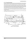
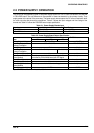
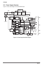
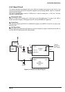
2.3 CONTROL CIRCUIT
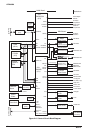
Figure 2-15 shows a block diagram of the control circuit with the C204 MAIN board at the center.
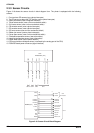
2.3.1 Control Circuit Operation Overview
The core of the control circuit is the TMP95C061AF CPU (IC2). This CPU is driven using a 24.57 MHz
external clock (CRU1). The CPU executes programs stored in the PROM (IC5). The CPU starts executing a
program upon receiving the reset signal from an external device (IC13) via the gate array E05B36 (IC1). The
CPU accesses the internal RAM and external RAM (IC14). The CPU also controls the EEPROM (IC11) used
to store the parameters, such as the tear off position, while the printer is turned off.
The CPU controls all the printer operations via the peripheral IC E05B36 (IC1) and controls the printer
mechanism. The main functions of the E05B36 (IC1) are: /CS (Chip Select) signal creation, address
decoding, printhead driver control, carriage driver control, encoder pulse circuit control, PG and HF phase
signal creation, interface control, CR and PF motor driver abnormal sensor circuit monitoring, reset signal
creation, control of the PSB/PSE board, control of the panel unit, and reading the DIP switch settings on the
C204 SUB board.
Signals, such as DRERR (driver error) and PD (power down), are connected to the C204 PSB/PSE board to
provide back-up control of the EEPROM (when the printer is turned off) and control of the power supply
voltage. When the POFF signal informs the CPU that the power has been turned off (or CL that the power
supply voltage has dropped), the CPU turns off the power supply voltage of the C204 PSB/PSE board by
outputting the PD signal.
The reset circuit outputs the reset signal when the printer is turned on or off, the voltage level drops, or a
reset signal is input from an external device. It resets the control circuit for a certain period directly or via the
E05B36.