


OPERATING PRINCIPLES
Rev. B
2-2
9
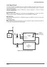
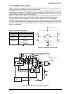
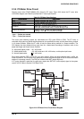
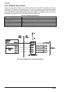
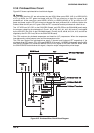
2.3.5 PF Motor Drive Circuit
Stepping motor driver STK6713BMK4 (IC2) drives the PF motor. Figure 2-22 shows the PF motor drive
circuit block diagram, and Table 2-9 provides the PF motor specifications.
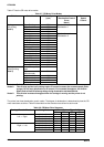
Table 2-9. PF Motor Specifications
Specification Description
Form 4-phase, 200-pole, HB* pulse motor
Supply Voltage 37 VDC (applied to the drive circuit)
Internal Coil Resistance 2.8 ohms + 10 % per phase at 25
o
C
Frequency 4274 pps** (normal mode,, constant driving): 9.9 ips***
2610 pps (middle speed mode,, constant driving): 6 ips
Current Consumption Driving: 1.75 A, + 0.20 A per phase (average)
Holding: 0.26 A, + 0. 2 A per phase (average)
*HB …. Hybrid
**pps …. pulses per second
***ips …. inches per second
The motor pulse switching signals are transmitted from CPU ports PG00 to PG03. The PF motor is
controlled using open-loop phase switching based on the specified time data, and the phase driving method
is 1-2 phase excitation. (When the PF motor is held, the phase driving method is 1 phase excitation.) The
CPU selects the most suitable driving mode from the modes below according to conditions such as the
paper feed length and the pull tractor condition.
Micro feed (adjust) mode : < 20 / 432 inches
Middle speed mode: > 20 / 432 inches and < 60 / 432 inches, or with optional pull tractor
Normal speed mode: > 60 / 432 inches
Each phase switching FET in driver IC2 is an open collector. When the phase switching data is HIGH, the
motor is turned on. The PFA port of the gate array monitors the phase A signal of the PF motor and checks
whether it is operating normally. The PFA port is used as the WDT (watch dog timer).
If PF motor operation is abnormal, the gate array outputs the /RSTOUT (reset request) signal to the system
reset IC (IC13). Refer to Section 2.3.2 Reset Circuit.
STK6713B
(IC2)
PF A
PF B
PF C
PF D
OUT_A
OUTXA
OUT_B
OUTXB
CPU TMP95C061A
(IC2)
PFH/R
PG00
PG01
PG02
PG03
VREF
VREF
PFA
+5V
GP3
4.3 VDC
Ref. Voltage
Setting Circuit (Q9)
IN_A
INXA
IN_B
INXB
GP3
SG
GP
Gate Array
E05B36 (IC1)
Vref
PF COM
VP3
DRV
Board
MAIN
Board
Figure 2-23. PF Motor Drive Circuit Block Diagram