


DFX-8500
Rev. B
2-1
6
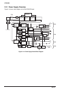
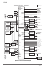
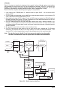
Protection circuits :
These +37VDC line blocks perform voltage control, and they have over-current limiting and over voltage
protection circuits for each.
Control and status signals :
The PSB//PSE board receives two control signal from the C204 MAIN board and outputs two status signals
to the MAIN board. Refer to Table 2-3 for the each signal and the printer status relationship.
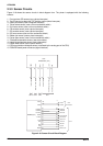
Fatal error recovery :
When the printer detects the fatal error, the PSB/PSE board cannot recover for APPROX.10 minutes by the
DRERR signal of the C204 MAIN board, after the power is turned off. Therefore, you must wait more than 10
minutes turn the power on again.
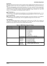
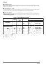
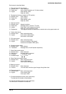
Table 2-4. PSB/PSE Board Control Signals
Signal In /
Out*1)
Signal Logic Function
Level Block 1*2) Block 2*3)
/PD
(Power Down)
In TTL High
Low
37 VDC
0 VDC
37 VDC, 5 VDC
37 VDC, 5 VDC
DRERR
(Head coil/driver error)
In TTL High
Low
0 VDC
37 VDC
0 VDC, 0 VDC
37 VDC, 5 VDC
/SD
(Source Down)
Out TTL High
Low
Indefiniteness
> 30 VDC, 5VDC
< 30 VDC, 5VDC
CL
(Current Limit*4)
Out TTL High
Low
37 VDC
< 35 VDC
37 VDC, 5 VDC
< 35 VDC, 5 VDC
*1): From the view of the PSB/PSE board.
*2): VP1-GP1 and VP2-GP2
*3): VP3-GP3 and +5V-GL
*4): Due to high duty printing