


OPERATING PRINCIPLES
Rev. B
2-21
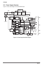
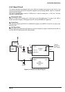
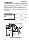
2.3.2 Reset Circuit
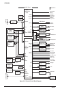
This section describes the hardware reset circuit. When the hardware reset signal is input, all ICs in the
control circuit are reset, and the CPU executes the program from the starting address. Figure 2-17 shows the
reset circuit block diagram.
The circuit is equipped with a reset IC: PTS591(IC13) is used for resetting the + 5 VDC line. The reset
operation is described below.
Power On/Off Reset:
Reset IC PTS591 (IC13) monitors the +5 VDC line on the C204 MAIN board. If it drops to 4.2 VDC or
smaller, the reset IC outputs a LOW signal to the CPU (IC2) and E05B36 (IC1) gate array.
Forced Reset:
The gate array outputs the RSTOUTX or ERRCRPFX signals to the XRESET of the CPU, and also to the
gate array itself.
/INIT Signal Reset:
When the gate array receives the /INIT signal from the host computer, the signal is transferred to the INT4 of
the CPU, then CPU performs the /INIT reset operation.
+5
1
30
XRESET
/RESETX
/RSTOUTX
Type-B,
Parallel I/F
/INIT signal
E05B36
(IC1)
CPU
TMP95C061
(IC2)
PST591
(IC13)
R218
C52
/ERRCRPFX
R215
C56
113
112
111
INITRQ
100
INT4
36
3
VOUT
VCC
Figure 2-17. Reset Circuit Block Diagram