Rev. 1.00, 05/04, page 356 of 544
123
KCLK
(pin state)
KD
(pin state)
KCLK
(input)
KCLK
(output)
KB7 to KB0
PER
KBS
KBF
Start
bit
Parity bit
Stop bit
Receive processing/
error handling
Automatic I/O inhibit
Previous data Receive data
Flag cleared
9
10 11
701
KB0 KB1
[1] [2] [3] [4] [5] [6]
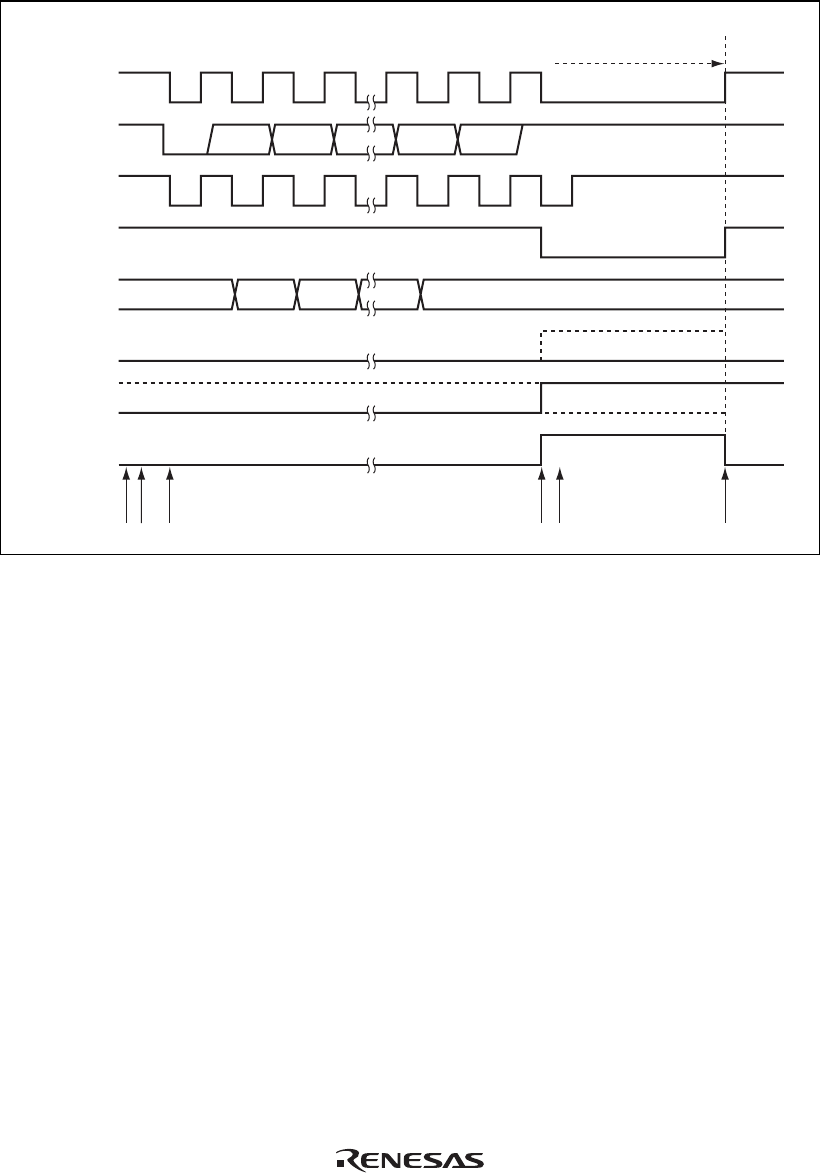
Figure 14.4 Receive Timing
14.4.2 Transmit Operation
In a transmit operation, KCLK (clock) is an output on the keyboard side, and KD (data) is an
output on the chip (system) side. KD outputs a start bit, 8 data bits (LSB-first), an odd parity bit,
and a stop bit, in that order. The KD value is valid when KCLK is high. A sample transmit
processing flowchart is shown in figure 14.5, and the transmit timing in figure 14.6.


