Rev. 1.00, 05/04, page 363 of 544
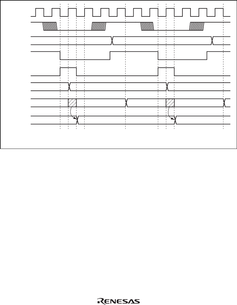
14.4.7 Receive Timing
Figure 14.12 shows the receive timing.
N + 1 N + 2N
KCLK (pin)
Note: * The φ clock shown here is scaled by 1/N in medium-speed mode when the operating mode is active
mode.
KD (pin)
Internal
KCLK (KCLKI)
Falling edge
signal
RXCR3 to
RXCR0
Internal KD
(KDI)
KBBR7 to
KBBR0
φ*
Figure 14.12 Receive Counter and KBBR Data Load Timing


