Rev. 1.00, 05/04, page 461 of 544
19.7 Clock Select Circuit
The clock select circuit selects the system clock that is used in this LSI.
A clock generated by an oscillator to which the EXTAL and XTAL pins are input is selected as a
system clock when returning from high-speed mode, medium-speed mode, sleep mode, reset state,
or standby mode.
A subclock input from the EXCL pin is selected as a system clock in subactive mode, subsleep
mode, or watch mode. At this time, modules such as the CPU, TMR_0, TMR_1, WDT_0,
WDT_1, ports, and interrupt controller and their functions operate depending on the φSUB. The
count clock and sampling clock for each timer are divided φSUB clocks.
19.8 Usage Notes
19.8.1 Note on Resonator
Since all kinds of characteristics of the resonator are closely related to the board design by the
user, use the example of resonator connection in this document for only reference; be sure to use
an resonator that has been sufficiently evaluated by the user. Consult with the resonator
manufacturer about the resonator circuit ratings which vary depending on the stray capacitances of
the resonator and installation circuit. Make sure the voltage applied to the oscillator pins does not
exceed the maximum rating.
19.8.2 Notes on Board Design
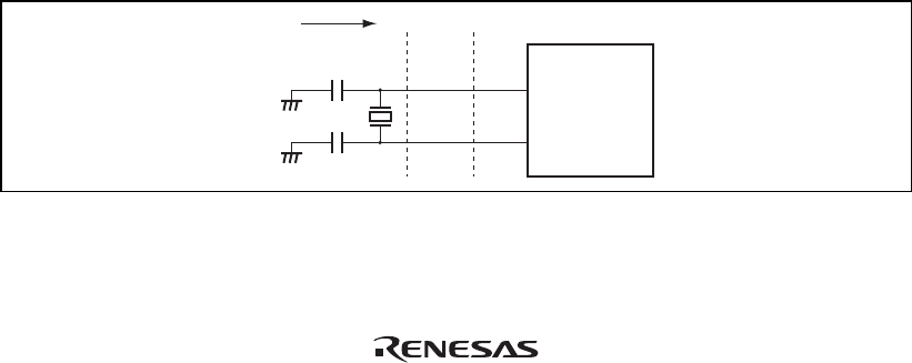
When using a crystal resonator, the crystal resonator and its load capacitors should be placed as
close as possible to the XTAL and EXTAL pins.
Other signal lines should be routed away from the oscillator circuit to prevent inductive
interference with the correct oscillation as shown in figure 19.8.
C
L2
Signal A Signal B
C
L1
This LSI
XTAL
EXTAL
Avoid
Figure 19.8 Note on Board Design of Oscillator Circuit Section


