


Intel
®
IXP43X Product Line of Network Processors
April 2007 HDG
Document Number: 316844; Revision: 001US 19
Hardware Design Guidelines—Intel
®
IXP43X Product Line of Network Processors
The memory controller only corrects single bit ECC errors on read cycles. The ECC is
stored into the DDRII/DDRI SDRAM array along with the data and is checked when the
data is read. If the code is incorrect, the MCU corrects the data before reaching the
initiator of the read. ECC error scrubbing is done with software. User-defined fault
correction software is responsible for The value written back into the memory location
contains the 32-bit word with the modified byte and the new ECC value.
Refer to the Intel
®
IXP43X Product Line of Network Processors Datasheet for a detailed
list of features.
General DDRII/I SDRAM routing guidelines can be found in Section 7.3.3, “Routing
Guidelines” on page 82. For more detailed information, see the PC266 and PC400 DDR
SDRAM specification.
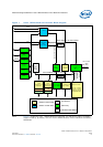
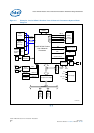
3.2.1 Signal Interface
Table 4. DDRII/I SDRAM Interface Pin Description (Sheet 1 of 2)
Name
Type
Field
Device-Pin Connection
VTT
Terminatio
n
Description
D_CK[2:0] /
DDR_CK[2:0]
O
Connect a pair of differential clock
signals to every device; When
using both banks, daisy chain
devices with same data bit
sequence.
No
DDRII/I SDRAM Clock Out — Provides the
positive differential clocks to the external
SDRAM memory subsystem.
D_CK_N[2:0] /
DDR_CK_N[2:0]
O Same as above No
DDRII/I SDRAM Clock Out — Provides the
negative differential clocks to the external
SDRAM memory subsystem.
D_CS_N[1:0] /
C_CS_N[1:0]
O
Use the same CS to control 32-bit
data + 8-bit ECC, per bank
Yes
Chip Select — Must be asserted for all
transactions to the DDRII/I SDRAM device.
One per bank.
D_RAS_N /
DDR_RAS_N
O
The RAS signal must be connected
to each device in a daisy chain
manner
Yes
Row Address Strobe — Indicates that the
current address on D_MA[13:0] /
DDR_MA[13:0] is the row.
D_CAS_N /
DDR_CAS_N
O
The CAS signal must be connected
to each device in a daisy chain
manner
Yes
Column Address Strobe — Indicates that the
current address on D_MA[13:0] /
DDR_MA[13:0] is the column.
D_WE_N / DDR_WE_N O
The WE signal must be connected
to each device in a daisy chain
manner
Yes
Write Strobe — Defines whether or not the
current operation by the DDRII/I SDRAM is to
be a read or a write.
D_DM[4:0] /
DDR_DM[4:0]
O
Connect to each DM device pin.
For the 8-bit devices connect one
DM signal per device.
For the 16-bit devices connect two
DM signal per device (depending
on how many data bits are being
used).
Yes
Data Bus Mask — Controls the DDRII/I SDRAM
data input buffers. Asserting D_WE_N/
DDR_WE_N causes the data on D_DQ[31:0]/
DDR_DQ[31:0] and D_CB[7:0]/DDR_CB[7:0]
to be written into the DDRII/I SDRAM devices.
D_DM[4:0]/DDR_DM[4:0] controls this
operation on a per-byte basis. D_DM[3:0]/
DDR_DM[3:0] are intended to correspond to
each byte of a word of data. D/DM[4]/
DDR_DM[4] is intended to be utilized for the
ECC byte of data.
D_BA[1:0] /
DDR_BA[1:0]
O
The BA signals must be connected
to each device in a daisy chain
manner.
Yes
DDRII/I SDRAM Bank Selects — Controls which
of the internal DDRII/I SDRAM banks to read
or write. D_BA[1:0]/DDR_BA[1:0] are used for
all technology types supported.
D_MA[13:0] /
DDR_MA[13:0]
O
All address signals must be
connected to each device in a
daisy chain manner.
Yes
Address bits 13 through 0 — Indicates the row
or column to access depending on the state of
D_RAS_N/DDR_RAS_N and D_CAS_N/
DDR_CAS_N.
D_DQ[31:0] /
DDR_DQ[31:0]
I/O
Must be connected in parallel to
achieve a 32-bit bus width.
Yes Data Bus — 32-bit wide data bus.