


Intel
®
IXP43X Product Line of Network Processors—Hardware Design Guidelines
Intel
®
IXP43X Product Line of Network Processors
HDG April 2007
80 Document Number: 316844; Revision: 001US
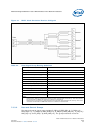
— Table 31 on page 79
Data Group to Strobe Summary:
• The more restrictive data group to strobe timing occurs for read operations
— Table 32 on page 80
— Table 33 on page 80
• The maximum allowable difference from any data group signal to the strobe is
±0.25 ns.
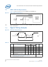
— Figure 30 on page 77
— Table 32 on page 80
Strobe to Clock Summary:
• The maximum allowable difference from any data strobe signal to the clock is -
0.475 ns to +0.875 ns
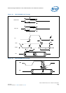
— Figure 32 on page 83
— Table 34 on page 83
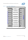
These are absolute maximum ratings for length mismatch based in ideal printed board
conditions (exact signal propagation delays, ideal signal integrity with no reflections or
settling, zero rise/fall times, and so on.). To compensate for these non-ideal conditions,
more restrictive length matching conditions should be used based on signal integrity
analysis and simulation to provide a buffer zone and avoid possible variations in silicon
or printed circuit board manufacture.
In addition to any trace length differentials which must be considered between signal
groups, differences in the package length between signals should be considered when
determining the total propagation delay of the signals. When using the IXP435
reference platform IBIS model for signal analysis, package characteristics are included
in the simulation results.
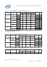
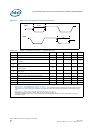
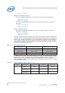
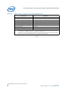
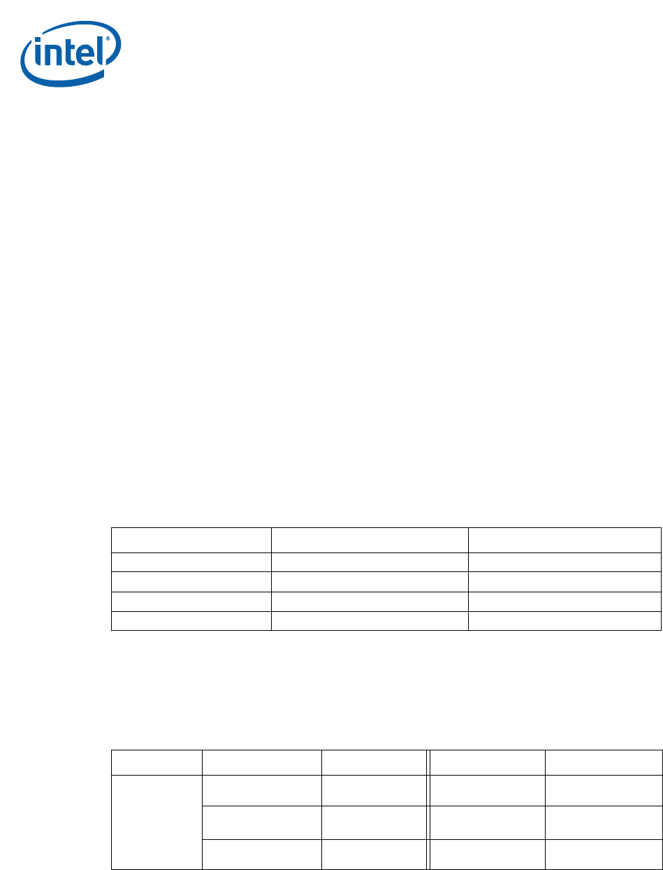
Table 32. Timing Relationships
Signal Group Absolute Minimum Length Absolute Maximum Length
Control to Clock Clock – 600 ps Clock + 600 ps
Command to Clock Clock – 600 ps Clock + 600 ps
Data to Strobe Strobe – 250 ps Strobe + 250 ps
Strobe to Clock Clock – 475 ps Clock + 875 ps
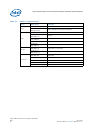
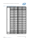
Table 33. Signal Package Lengths (Sheet 1 of 3)
Group Signal Name Length (mil) Signal Name Length (mil)
Clock
D_CK_N0 /
DDR_CK_N0
558.19 D_CK0 / DDR_CK0 507.46
D_CK_N1 /
DDR_CK_N1
385.12 D_CK1 / DDR_CK1 385.12
D_CK_N2 /
DDR_CK_N2
504.20 D_CK2 / DDR_CK2 548.01