


Intel
®
IXP43X Product Line of Network Processors
April 2007 HDG
Document Number: 316844; Revision: 001US 3
Hardware Design Guidelines—Intel
®
IXP43X Product Line of Network Processors
Contents
1.0 Introduction ..............................................................................................................9
1.1 Content Overview................................................................................................9
1.2 Related Documentation ...................................................................................... 10
1.3 Acronyms......................................................................................................... 10
1.4 Overview ......................................................................................................... 11
1.5 Typical Applications ........................................................................................... 14
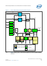
2.0 System Architecture ................................................................................................ 15
2.1 System Architecture Description.......................................................................... 15
2.2 System Memory Map ......................................................................................... 15
3.0 General Hardware Design Considerations ................................................................ 17
3.1 Soft Fusible Features ......................................................................................... 17
3.2 DDRII/I SDRAM Interface ................................................................................... 18
3.2.1 Signal Interface ..................................................................................... 19
3.2.2 DDRII/I SDRAM Initialization ................................................................... 20
3.3 Expansion Bus .................................................................................................. 21
3.3.1 Signal Interface ..................................................................................... 21
3.3.2 Reset Configuration Straps ...................................................................... 22
3.3.3 8-Bit Device Interface............................................................................. 24
3.3.4 16-Bit Device Interface ........................................................................... 25
3.3.5 Flash Interface....................................................................................... 26
3.4 UART Interface ................................................................................................. 26
3.4.1 Signal Interface ..................................................................................... 27
3.5 MII Interface .................................................................................................... 28
3.5.1 Signal Interface MII................................................................................ 29
3.5.2 Device Connection, MII ........................................................................... 30
3.6 GPIO Interface.................................................................................................. 31
3.6.1 Signal Interface ..................................................................................... 32
3.6.2 Design Notes ......................................................................................... 32
3.7 USB Interface ................................................................................................... 32
3.7.1 Signal Interface ..................................................................................... 33
3.8 UTOPIA Level 2 Interface ................................................................................... 36
3.8.1 Signal Interface ..................................................................................... 36
3.8.2 Device Connection.................................................................................. 40
3.9 HSS Interface ................................................................................................... 40
3.9.1 Signal Interface ..................................................................................... 41
3.9.2 Device Connection.................................................................................. 41
3.10 SSP Interface ................................................................................................... 42
3.10.1 Signal Interface ..................................................................................... 43
3.10.2 Device Connection.................................................................................. 43
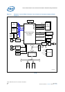
3.11 PCI Interface .................................................................................................... 44
3.11.1 Signal Interface ..................................................................................... 45
3.11.2 PCI Interface Block Diagram .................................................................... 46
3.11.3 PCI Option Interface ............................................................................... 47
3.11.4 Design Notes ......................................................................................... 49
3.12 JTAG Interface.................................................................................................. 49
3.12.1 Signal Interface ..................................................................................... 50
3.13 Input System Clock ........................................................................................... 50
3.13.1 Clock Signals ......................................................................................... 50
3.13.2 Clock Oscillator ...................................................................................... 50
3.13.3 Recommendations for Crystal Selection ..................................................... 51