


Intel
®
IXP43X Product Line of Network Processors—Hardware Design Guidelines
Intel
®
IXP43X Product Line of Network Processors
HDG April 2007
78 Document Number: 316844; Revision: 001US
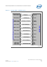
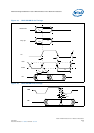
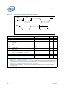
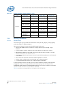
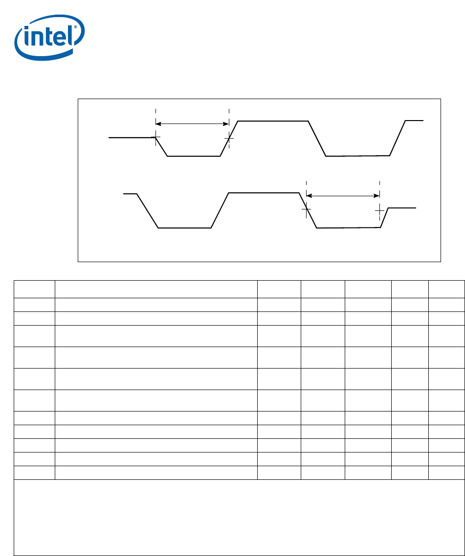
Figure 31. DDR - Write Preamble/Postamble Duration
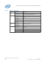
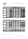
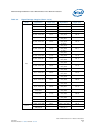
Table 30. DDRII-400 MHz Interface -- Signal Timings
Symbol Parameter Minimum Nominal Maximum Units Notes
T
VB1
DQ, CB and DM write output valid time before DQS. 521 ps 1
T
VA1
DQ, CB and DM write output valid time after DQS. 521 ps 1
T
VB3
Address and Command write output valid before CK
rising edge.
1771 ps 1, 4
T
VA3
Address and Command write output valid after CK rising
edge.
1771 ps 1, 4
T
VB4
DQ, CB and DM read input valid time before DQS rising
or falling edges.
323 ps 2
T
VA4
DQ, CB and DM read input valid time after DQS rising or
falling edges.
323 ps 2
T
VB5
CS_N[1:0] control valid before CK rising edge. 1771 ps 4
T
VA5
CS_N[1:0] control valid after CK rising edge. 1771 ps 4
T
VB6
DQS write preamble duration. 3750 ps 3
T
VA6
DQS write postamble duration. 2500 ps 3
T
V7
DQ, CB, and DM pulse width (tDIPW) 1750 ps 1
Notes:
1. See Figure 29, “DDR SDRAM Write Timings” on page 77
2. See Figure 30, “DDR SDRAM Read Timings” on page 77. The specified minimum requirements for the “Data to strobe
read setup” and “Data from strobe read hold” are determined with the DQS delay programmed for 90 degree phase
shift.
3. See Figure 31, “DDR - Write Preamble/Postamble Duration” on page 78
4. Address/Command pin group; RAS_N, CAS_N, WE_N, MA[13:0], BA[1:0]
5. Designed to JEDEC specification; it is recommended that IBIS models should be used to verify signal integrity on
individual designs
DQS
T
VB6
DQS
T
VA6