


Intel
®
IXP43X Product Line of Network Processors—Hardware Design Guidelines
Intel
®
IXP43X Product Line of Network Processors
HDG April 2007
50 Document Number: 316844; Revision: 001US
3.11.4 Design Notes
• The IXP43X network processors do not support the 5 V PCI signal interface by
itself. Only the 3.3 V signal interface is supported without signal level conversion;
however, it is possible to interface to 5 V logic while using a voltage level converter.
•The PCI Local Bus Specification, Rev. 2.2 requires that the bus is always parked,
as some device is always driving the AD lines. You must use pull-ups on these
signals. The specification states that the following control lines should be pulled up:
• The GPIO pins of the IXP43X network processors
can be used by PCI devices on PCI
slots to request an interrupt from the processors’ PCI controller.
• PCI_INTA_N is used to request interrupts to external PCI Masters. This signal is an
open drain and requires a pull-up resistor.
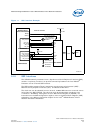
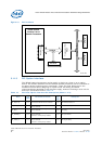
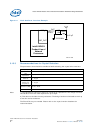
3.12 JTAG Interface
JTAG is the popular name for IEEE standards 1149.1-1990 and 1149.1a-1993, IEEE
Standard Test Access Port and Boundary-Scan Architecture, which provides support
for:
• Board-level boundary-scan connectivity testing
• Connection to software debugging tools through the JTAG interface
• In-system programming of programmable memory and logic devices on the PCB
The interface is controlled through five dedicated test access port (TAP) pins: TDI, TMS,
TCK, nTRST, and TDO, as described in the IEEE 1149.1 standard. The boundary-scan
test-logic elements include the TAP pins, TAP controller, instruction register,
boundary-scan register, bypass register, device identification register, and data-specific
registers. These are described in the Intel
®
IXP43X Product Line of Network Processors
Developer’s Manual.
The IXP43X network processors can be controlled during debug through a JTAG
interface to the processor, the debug tools such as the Macraigor Systems Raven*, EPI
Majic*, Wind River Systems* visionPROBE*/ visionICE* or various other JTAG tools
plug into the JTAG interface through a connector.
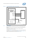
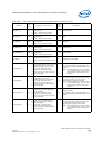
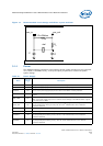
PCI_INTA_N O/D
Connect PCI_INTA_N output from the
Option to one of the GPIO input signals
of the Host. The GPIO signal at the
Host must be configure as an input
interrupt level sensitive.
O/D
Interrupt A
This interrupt is generated from the Option to
one of the GPIO inputs to the Host.
On the Host this signal is not used, it should
be pulled high with a 10-KΩ resistor.
PCI_CLKIN I
Clock must be connected to both
devices. Trace lengths must be
matched. Use point to point clock
distribution.
IClock input
Table 18. PCI Host/Option Interface Pin Description (Sheet 3 of 3)
Name
Type
Field
Device-Pin Connection
Option
Type
Field
Description
—FRAME_N —TRDY_N —IRDY_N —DEVSEL_N
— STOP_N — SERR_N — PERR_N — LOCK_N
—INTA_N —INTB_N —INTC_N —INTD_N