


Intel
®
IXP43X Product Line of Network Processors—Hardware Design Guidelines
Intel
®
IXP43X Product Line of Network Processors
HDG April 2007
20 Document Number: 316844; Revision: 001US
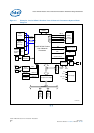
3.2.2 DDRII/I SDRAM Initialization
For instructions on DDRII/I SDRAM initialization, refer to DDR SDRAM Initialization
subsection in the Memory Controller chapter of the Intel
®
IXP43X Product Line of
Network Processors Developer’s Manual.
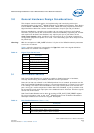
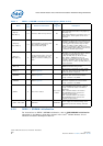
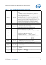
D_CB[7:0] /
DDR_CB[7:0]
I/O Connect to ECC memory devices. Yes
ECC Bus — Eight-bit error correction code
which accompanies the data on D_DQ[31:0]/
DDR_DQ[31:0].
When ECC is disabled and not being used in a
system design, these signals can be left un-
connected.
D_DQS[4:0] /
DDR_DQS[4:0]
I/O
Connect DQS[3:0] to devices with
data signals and DQS[4] to
devices with ECC signals.
Yes
Data Strobes Differential — Strobes that
accompany the data to be read or written from
the DDRII/I SDRAM devices. Data is sampled
on the negative and positive edges of these
strobes. D_DQS[3:0]/DDR_DQS[3:0] are
intended to correspond to each byte of a word
of data. D_DQS[4]/DDR_DQS[4] is intended to
be utilized for the ECC byte of data.
D_CKE[1:0] /
DDR_CKE[1:0]
O
Use one CKE per bank, never mix
the CKE on the same bank. Use
CKE[0] for bank0 and CKE[1] for
bank1
Yes
Clock enables — One clock after D_CKE[1:0]/
DDR_CKE[1:0] is de-asserted, data is latched
on D_DQ[31:0]/DDR_DQ[31:0] and
D_CB[7:0]/DDR_CB[7:0]. Burst counters
within DDRII/I SDRAM device are not
incremented. De-asserting this signal places
the DDRII/I SDRAM in self-refresh mode. For
normal operation, D_CKE[1:0]/DDR_CKE[1:0]
must be asserted.
D_ODT[1:0]
On Die Termination Control — Turns on DDR II
SDRAM termination during writes.
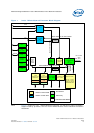
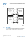
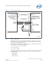
D_RES[2:1] Refer to Figure 27
Compensation for DDR OCD (analog) DDRII
mode only. This function is not enable and
special connection is required.
D_SLWCRES Refer to Figure 27
Compensation Voltage Reference (analog) for
DDR driver slew rate control connected
through a resistor to D_CRES0.
D_IMPCRES Refer to Figure 27
Compensation Voltage Reference (analog) for
DDR driver impedance control connected
through a resistor to D_CRES0.
D_CRES0 O Tied off to a resistor
Tied off to a
resistor
Analog VSS Ref Pin (analog) both D_SLWCRES
and D_IMPCRES signals connect to this pin
through a reference resistor. For DDRII/I
respectively:
- 285 / 387Ohm Resistor connected to
DDR_IMPCRES used for process and
temperature adjustments.
- 825 / 845Ohm Resistor connected to
DDR_SLWCRES used for process and
temperature adjustments.
D_VREF / DDR_VREF I VCCDDR/2 VCCDDR/2
DDRII/IDDRII/I SDRAM Voltage Reference — is
used to supply the reference voltage to the
differential inputs of the memory controller
pins.
Table 4. DDRII/I SDRAM Interface Pin Description (Sheet 2 of 2)
Name
Type
Field
Device-Pin Connection
VTT
Terminatio
n
Description