Intel
®
IXP43X Product Line of Network Processors
April 2007 HDG
Document Number: 316844; Revision: 001US 83
Hardware Design Guidelines—Intel
®
IXP43X Product Line of Network Processors
7.3.3.2 Data and Control Groups
The data and control signal group includes D_CB[7:0]/DDR_CB[7:0], D_DQ[31:0] /
DDR_DQ[31:0], D_DQS[4:0]/DDR_DQS[4:0], D_DM[4:0]/DDR_DM[4:0]., D_CS[1:0]/
DDR_CS[1:0] and D_CKE[1:0]/DDR_CKE[1:0]. The groups should be routed on
Figure 32. DDRII Clock Simulation Results: CK Signals
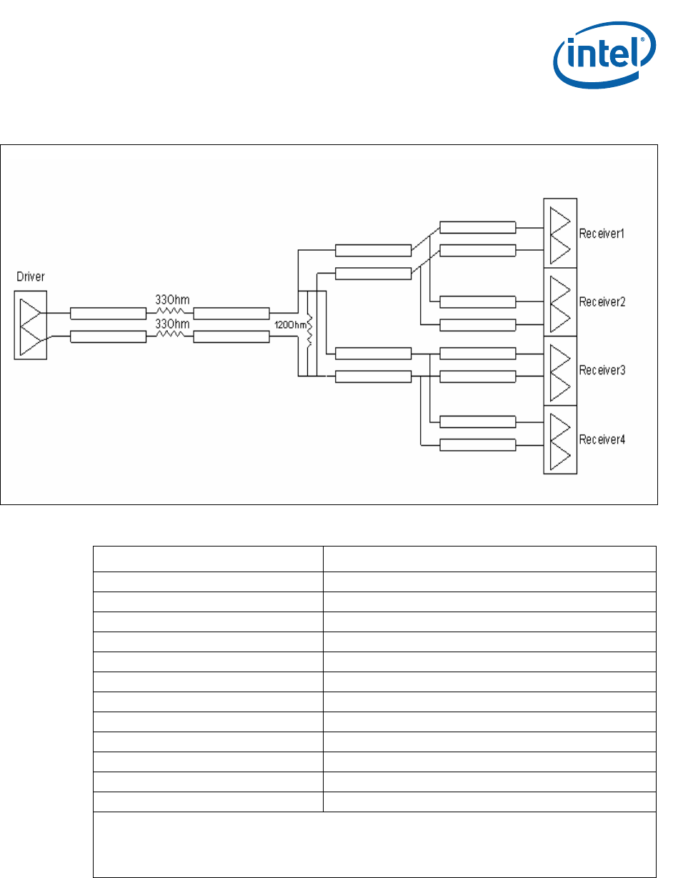
Table 34. Clock Signal Group Routing Guidelines
Parameter Definition
Signal Group Members D_CK[2:0] and D_CK_N[2:0]
Topology Differential Pair Point to Point (1 Driver, 4 Receivers)
Single Ended Trace Impedance (Z
o
) 50 Ω
Series Resistor 33 Ω
Nominal Trace Width
1
Internal (Strip Line) 3.5 mils, External (Micro Strip) 5 mils
Nominal Pair Spacing (edge to edge)
2
Internal (Strip Line) 10.5 mils, External (Micro Strip) 10 mils
Minimum Pair to Pair Spacing Any layer 20mils
Minimum Spacing to Other DDR Signals 20.0 mils
Minimum Spacing to non-DDR Signals 25.0 mils
Maximum Via Count 5 per trace
Total Trace Length 500 mils to 1000 mils
DDR_CK to DDR_CK_N Length Matching Match total length to +/- 10 mils between clocks
Notes:
1. Nominal trace width is determined by board physical characteristics and stack-up. This value should
be verified with the PWB manufacturer to achieve the desired Zo.
2. Nominal pair to pair spacing is determined by board physical characteristics and stack-up. This value
should be verified with the PWB manufacturer to achieve the desired Zdiff.


