


Intel
®
IXP43X Product Line of Network Processors—Hardware Design Guidelines
Intel
®
IXP43X Product Line of Network Processors
HDG April 2007
76 Document Number: 316844; Revision: 001US
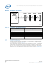
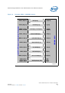
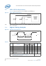
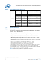
7.3 DDRII OCD Pin Requirements
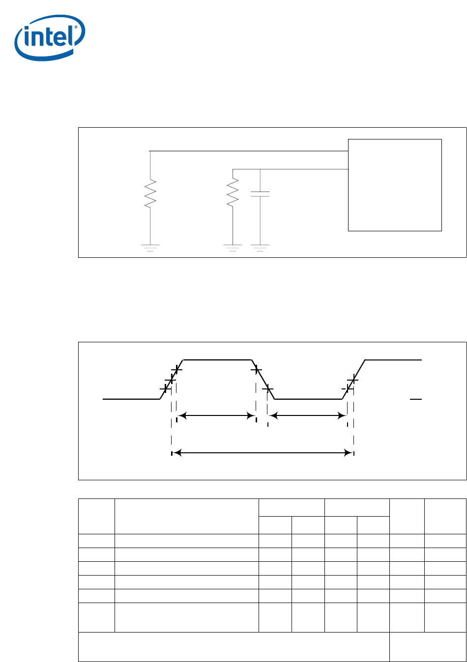
Figure 27 shows the requirement for the DDRRES1 and DDRRES2 pins.
Note: Since the OCD calibration function is not enabled, DDRRES2 must be pulled to ground
with a 1-KΩ resistor.
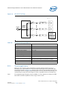
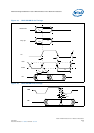
7.3.1 Signal-Timing Analysis
Figure 27. DDRII OCD Pin Requirements
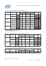
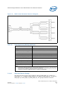
Figure 28. DDR Clock Timing Waveform
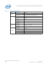
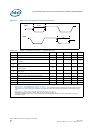
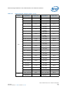
Table 29. DDR Clock Timings
Symbol Parameter
DDR-II 400 DDR-I 266
Units Notes
Min Max Min Max
T
F
DDR SDRAM clock Frequency 200 133 MHz
T
C
DDR SDRAM clock Cycle Time 5 7.5 ns 1
T
CH
DDR SDRAM clock High Time 2.15 3.37 ns 1
T
CL
DDR SDRAM clock Low Time 2.15 3.37 ns 1
T
CS
DDR SDRAM clock Period Stability 350 350 ps
T
skew
DDR SDRAM clock skew for any
differential clock pair (D_CK[2:0] -
D_CK_N[2:0])
100 100 ps
Notes:
1. See Figure 28, “DDR Clock Timing Waveform” on page 76
2. Vtest is nominally (0.5 * Vtch - Vtcl)
Intel® IXP43X
Product Line
of Network
Processors
DDRRES2
DDRRES1
40.2
Ω
resistor
1K
Ω
resistor
0. 1 uF
T
CH
T
CL
T
C
V
tch
V
ih(min)
V
il(max)
V
test
V
tcl
V
ih(min)
V
il(max )
V
il(max )
V
test