


Intel
®
IXP43X Product Line of Network Processors
April 2007 HDG
Document Number: 316844; Revision: 001US 23
Hardware Design Guidelines—Intel
®
IXP43X Product Line of Network Processors
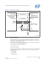
EX_ADDR[10] IOWAIT_CS0
1 = EX_IOWAIT_N is sampled during the read/write expansion bus cycles for Chip
Select 0.
0 = EX_IOWAIT_N is ignored for read and write cycles to Chip select 0 if
EXP_TIMING_CS0 is configured to Intel mode that is mentioned in Intel
®
IXP43X
Product Line of Network Processors Datasheet and Intel
®
IXP43X Product Line of
Network Processors Developer’s Manual.
Typically, IOWAIT_CS0 must be pulled down to Vss when attaching a Synchronous
Intel StrataFlash
®
on Chip Select 0 since the default mode for EXP_TIMING_CS0 is
Intel mode and EX_IOWAIT_N is an unknown value for Synchronous Intel
StrataFlash.
If the board does not connect the Synchronous Intel StrataFlash WAIT pin to
EX_WAIT_N (and the board guarantees EX_IOWAIT_N is pulled up), the value of
IOWAIT_CS0 is a don’t-care, since EX_IOWAIT_N will not be asserted.
When EXP_TIMING_CS0 is reconfigured to Intel Synchronous mode during
boot-up (for synchronous Intel chips), the expansion bus controller ignores
EX_IOWAIT_N during read and write cycles since the WAIT functionality is
determined from the EXP_SYNCINTEL_COUNT and EXP_TIMING_CS registers.
EX_ADDR[9] EXP_MEM_DRIVE Refer to table found in EX_ADDR[5].
EX_ADDR[8] USB Clock
Controls the USB clock select.
1 = USB Host/Device clock is generated internally
0 = USB Device clock is generated from GPIO[0].
When generating a spread spectrum clock on OSC_IN, GPIO[1] can be driven from
the system board to generate a 48 MHz clock for the USB Host.
EX_ADDR[7] 32_FLASH
Selects the data bus width of the FLASH memory device found on Chip Select 0.
Refer to 8/16_FLASH bit (Bit 0) of this register as well.
0 = 8 or 16-bit data bus size (must be pulled down during address strapping)
1 = not supported
EX_ADDR[6] (Reserved) (Reserved)
EX_ADDR[5] EXP_DRIVE
Expansion bus low/medium/high drive strength. The drive strength depends on
EXP_DRIVE and EXP_MEM_DRIVE configuration bits.
EXP_MEM_DRIVE EXP_DRIVE Expansion drive strength
------------------------------------------------------------------------------------
0 0 Reserved
0 1 Medium Drive
1 0 Low Drive
1 1 High Drive
EX_ADDR[4] PCI_CLK
Sets the clock speed of the PCI Interface
0 = 33 MHz (must be pulled down during address strapping)
1 = not supported
EX_ADDR[3] (Reserved)
(Reserved). EX_ADDR[3] must not be pulled down during address strapping. This
bit must be written to ‘1’ if performing a write to this register.
EX_ADDR[2] PCI_ARB
Enables the PCI Controller Arbiter
0 = PCI arbiter disabled
1 = PCI arbiter enabled
EX_ADDR[1] PCI_HOST
Configures the PCI Controller as PCI Bus Host
0 = PCI as non-host
1 = PCI as host
EX_ADDR[0] 8/16_FLASH
Specifies the data bus width of the FLASH memory device found on Chip Select 0.
8/16_FLASH Data bus size
0 16-bit
1 8-bit
Table 6. Boot/Reset Strapping Configuration (Sheet 2 of 2)
Name Function Description