


Intel
®
IXP43X Product Line of Network Processors
April 2007 HDG
Document Number: 316844; Revision: 001US 71
Hardware Design Guidelines—Intel
®
IXP43X Product Line of Network Processors
7.0 DDRII / DDRI SDRAM
7.1 Introduction
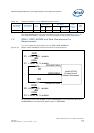
This document is intended to be used as a guide for routing DDRII/DDRI SDRAM based
on the Intel
®
IXP435 Multi-Service Residential Gateway Reference Platform. It contains
routing guidelines and simulation results for using x16 Thin Small Outline Package
(TSOP) memory devices soldered onto the processor module.
The memory controller only corrects single bit ECC errors on read cycles. The ECC is
stored into the DDRII/DDRI SDRAM array along with the data and is checked when the
data is read. If the code is incorrect, the MCU corrects the data before reaching the
initiator of the read. ECC error scrubbing is done with software. User-defined fault
correction software is responsible for scrubbing the memory array and handling double-
bit errors.
To limit double-bit errors from occurring, periodically read the entire usable memory
array to allow the hardware unit within the memory controller to correct any single-bit.
This also prevents the ECC errors that would have occurred prior to these errors
becoming double-bit ECC errors. Implementing this method is system-dependent.
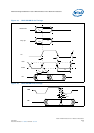
Note: It is important to note that when sub-word writes (byte writes or half-word writes
within a word-aligned boundary) are done to a 32-bit memory with ECC enabled, the
memory controller performs read-modify writes. There is a performance impact with
read-modify writes that must be considered when writing software.
With read-modify writes, the memory controller reads the 32-bit word that
encompasses the byte that is to be written when a byte write is requested. The
memory controller modifies the specified byte, calculates a new ECC, and writes the
entire 32-bit word back into the memory location it was read from.
The value written back into the memory location contains the 32-bit word with the
modified byte and the new ECC value.
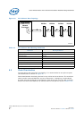
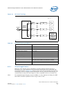
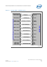
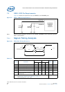
The MCU supports two physical banks of DDRII/DDRI SDRAM. The MCU has support for
unbuffered DDRI 266 and DDRII 400 in the form of discrete chips only.
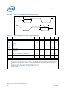
The MCU supports a memory subsystem ranging from 32 MB to 1 GB for 32-bit
memory systems for DDRI SDRAM, from 64 MB to 512 MB for 32-bit memory systems
for DDRII SDRAM, and supports 16 MB for 16-bit memory systems for DDRI SDRAM
(non-ECC), and 32 MB for 16-bit memory systems for DDRII SDRAM (non-ECC). An
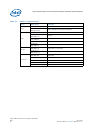
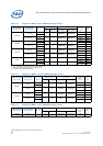
ECC or non-ECC system can be implemented using x8, or x16 devices. Table 25,
Table 26, Table 27 and Table 28 illustrate the supported DDRII/DDRI SDRAM
configurations
The two DDRII/DDRI SDRAM chip enables (DDR_CS_N[1:0]) support a DDRII/DDRI
SDRAM memory subsystem consisting of two banks. The base address for the two
contiguous banks are programmed in the DDRII/DDRI SDRAM Base Register (SDBR)
and is aligned to a 16 MB boundary. The size of each DDRII/DDRI SDRAM bank is
programmed with the DDRII/DDRI SDRAM boundary registers (SBR0 and SBR1).
The DDRII/DDRI SDRAM devices comprise four internal leaves. The MCU controls the
leaf selects within DDRII/DDRI SDRAM by toggling DDR_BA[0] and DDR_BA[1].