


Intel
®
IXP43X Product Line of Network Processors—Hardware Design Guidelines
Intel
®
IXP43X Product Line of Network Processors
HDG April 2007
4 Document Number: 316844; Revision: 001US
3.14 Power ..............................................................................................................52
3.14.1 Decoupling Capacitance Recommendations.................................................53
3.14.2 VCC Decoupling......................................................................................53
3.14.3 VCC33 Decoupling ..................................................................................53
3.14.4 VCCDDR Decoupling................................................................................53
3.14.5 Power Sequence .....................................................................................53
3.14.6 Reset Timing..........................................................................................53
4.0 General PCB Guide ...................................................................................................55
4.1 PCB Overview ...................................................................................................55
4.2 General Recommendations..................................................................................55
4.3 Component Selection .........................................................................................55
4.4 Component Placement........................................................................................55
4.5 Stack-Up Selection.............................................................................................56
5.0 General Layout and Routing Guide ...........................................................................59
5.1 Overview..........................................................................................................59
5.2 General Layout Guidelines...................................................................................59
5.2.1 General Component Spacing ....................................................................60
5.2.2 Clock Signal Considerations......................................................................62
5.2.3 MII Signal Considerations ........................................................................63
5.2.4 USB V2.0 Considerations .........................................................................63
5.2.5 Crosstalk ...............................................................................................63
5.2.6 EMI Design Considerations.......................................................................64
5.2.7 Trace Impedance....................................................................................64
5.2.8 Power and Ground Plane..........................................................................64
6.0 PCI Interface Design Considerations........................................................................66
6.1 Electrical Interface.............................................................................................66
6.2 Topology ..........................................................................................................66
6.3 Clock Distribution ..............................................................................................67
6.3.1 Trace Length Limits.................................................................................68
6.3.2 Routing Guidelines..................................................................................69
6.3.3 Signal Loading........................................................................................69
7.0 DDRII / DDRI SDRAM ..............................................................................................70
7.1 Introduction......................................................................................................70
7.2 DDRII/DDRI RCOMP and Slew Resistances Pin Requirements...................................74
7.3 DDRII OCD Pin Requirements..............................................................................75
7.3.1 Signal-Timing Analysis ............................................................................75
7.3.2 Timing Relationships ...............................................................................78
7.3.3 Routing Guidelines..................................................................................81
7.3.3.1 Clock Group..............................................................................81
7.3.3.2 Data and Control Groups............................................................82
7.3.3.3 Command Groups .....................................................................84
Figures
1Intel
®
IXP435 Network Processor Block Diagram ..........................................................13
2Example: Intel
®
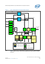
IXP43X Product Line of Network Processors System Block Diagram..........16
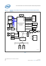
3 8/16-Bit Device Interface ..........................................................................................25
4 Flash Interface Example ............................................................................................26
5 UART Interface Example............................................................................................28
6 MII Interface Example...............................................................................................31
7 Common Mode Choke ...............................................................................................34
8 USB RCOMP and ICOMP Pin Requirement.....................................................................35
9 USB Host Down Stream Interface Example...................................................................35
10 UTOPIA Interface Example.........................................................................................40