


Intel
®
IXP43X Product Line of Network Processors—Hardware Design Guidelines
Intel
®
IXP43X Product Line of Network Processors
HDG April 2007
84 Document Number: 316844; Revision: 001US
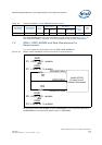
internal layers, except for pin escapes. It is recommended that pin escape vias be
located directly adjacent to the ball pads on all signals. Surface layer routing should be
minimized. The following table provides routing guidelines for signals within these
groups.
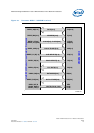
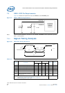
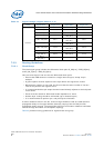
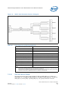
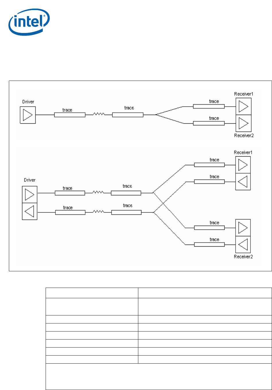
Figure 33. DDRII Data and Control Simulation Results: DQ and DQS signals
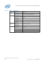
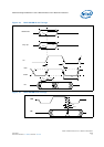
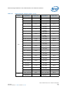
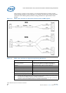
Table 35. DDRII Data and Control Signal Group Routing Guidelines
Parameter Definition
Signal Group Members
D_CB[7:0]/DDR_CB[7:0], D_DQ[31:0] / DDR_DQ[31:0],
D_DQS[4:0]/DDR_DQS[4:0], D_DM[4:0]/DDR_DM[4:0].,
D_CS[1:0]/DDR_CS[1:0] and D_CKE[1:0]/DDR_CKE[1:0]
Topology Differential Pair Point to Point (1 Driver, 2 Receivers)
Single Ended Trace Impedance (Z
o
)50 Ω
Series Resistor 22 Ω
Nominal Trace Width
1
Internal (Strip Line) 3.5 mils, External (Micro Strip) 5 mils
Nominal Pair Spacing (edge to edge)
2
Internal (Strip Line) 10.5 mils, External (Micro Strip) 10 mils
Minimum Pair to Pair Spacing Any layer 20mils
Notes:
1. Nominal trace width is determined by board physical characteristics and stack-up. This value should
be verified with the PWB manufacturer to achieve the desired Zo.
2. Nominal pair to pair spacing is determined by board physical characteristics and stack-up. This value
should be verified with the PWB manufacturer to achieve the desired Zdiff.
DQ
22 ohm
DQ
22 ohm
DQSDQS