S/UNI-QUAD
PMC-Sierra, Inc.
PM5349 S/UNI-QUAD
DATASHEET
PMC-971239 ISSUE 6 SATURN USER NETWORK INTERFACE (155-QUAD)
Proprietary and Confidential to PMC-Sierra, Inc., and for its Customers’ Internal Use
12
9
PIN DESCRIPTION
9.1
Line Side Interface Signals
Pin Name Type Pin
No.
Function
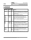
REFCLK Input AC5 The reference clock input (REFCLK) must provide a
jitter-free 19.44 MHz reference clock. It is used as
the reference clock by both clock recovery and clock
synthesis circuits.
This pin is shared by all channels.
RXD1+
RXD1-
RXD2+
RXD2-
RXD3+
RXD3-
RXD4+
RXD4-
Differential
PECL
inputs
E2
D1
G1
G2
W1
V2
AA1
Y2
The receive differential data inputs (RXD+, RXD-)
contain the NRZ bit serial receive stream. The
receive clock is recovered from the RXD+/- bit
stream. Please refer to the Operation section for a
discussion of PECL interfacing issues.
This pin is available independently for each channel.
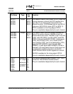
SD1
SD2
SD3
SD4
Single-
Ended
PECL
Input
E3
J3
U3
W3
The Signal Detect pin (SD) indicates the presence
of valid receive signal power from the Optical
Physical Medium Dependent Device. A PECL high
indicates the presence of valid data and a PECL low
indicates a loss of signal. It is mandatory that SD be
terminated into the equivalent network that RXD+/-
is terminated into.
This pin is available independently for each channel.
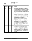
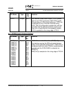
RCLK1
RCLK2
RCLK3
RCLK4
Output AA13
Y13
AC14
AB14
The receive byte clock (RCLK) provides a timing
reference for the S/UNI-QUAD receive outputs.
RCLK is a divide by eight of the recovered line rate
clock (19.44 MHz).
This pin is available independently for each channel.


