S/UNI-QUAD
PMC-Sierra, Inc.
PM5349 S/UNI-QUAD
DATASHEET
PMC-971239 ISSUE 6 SATURN USER NETWORK INTERFACE (155-QUAD)
Proprietary and Confidential to PMC-Sierra, Inc., and for its Customers’ Internal Use
23
9.3
Microprocessor Interface Signals
Pin Name Type Pin
No.
Function
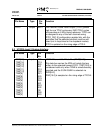
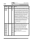
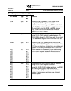
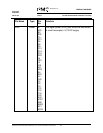
CSB Input B11 The active-low chip select (CSB) signal is low
during S/UNI-QUAD register accesses.
Note that when not being used, CSB must be tied
high. If CSB is not required (i.e., registers accesses
are controlled using the RDB and WRB signals
only), CSB must be connected to an inverted
version of the RSTB input.
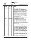
RDB Input D11 The active-low read enable (RDB) signal is low
during S/UNI-QUAD register read accesses. The
S/UNI-QUAD drives the D[7:0] bus with the contents
of the addressed register while RDB and CSB are
low.
WRB Input A10 The active-low write strobe (WRB) signal is low
during a S/UNI-QUAD register write accesses. The
D[7:0] bus contents are clocked into the addressed
register on the rising WRB edge while CSB is low.
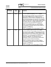
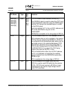
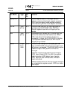
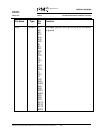
D[0]
D[1]
D[2]
D[3]
D[4]
D[5]
D[6]
D[7]
I/O D16
B17
A17
C16
B16
C15
B15
D14
The bi-directional data bus D[7:0] is used during
S/UNI-QUAD register read and write accesses.
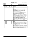
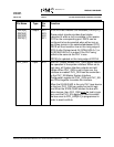
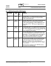
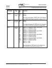
A[0]
A[1]
A[2]
A[3]
A[4]
A[5]
A[6]
A[7]
A[8]
A[9]
Input A15
C14
B14
A14
D13
C13
B13
A13
C12
B12
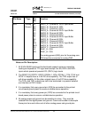
The address bus A[9:0] selects specific registers
during S/UNI-QUAD register accesses.
Except for S/UNI-QUAD global registers, the A[9:8]
bits allow to select which channel is being
accessed. The A[7:0] bits allow to select which
register is being access within a given channel
address space.


