S/UNI-QUAD
PMC-Sierra, Inc.
PM5349 S/UNI-QUAD
DATASHEET
PMC-971239 ISSUE 6 SATURN USER NETWORK INTERFACE (155-QUAD)
Proprietary and Confidential to PMC-Sierra, Inc., and for its Customers’ Internal Use
196
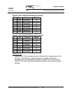
Addr Bit 7 Bit 6 Bit 5 Bit 4 Bit 3 Bit 2 Bit 1 Bit 0
8BH
8CH
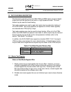
The following inputs cannot be read using the IOTST feature: D[7:0], A[7:0], ALE,
CSB, WRB, RDB, RSTB, TRSTB, TMS, TCK, and TDI.
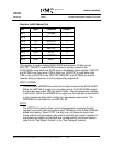
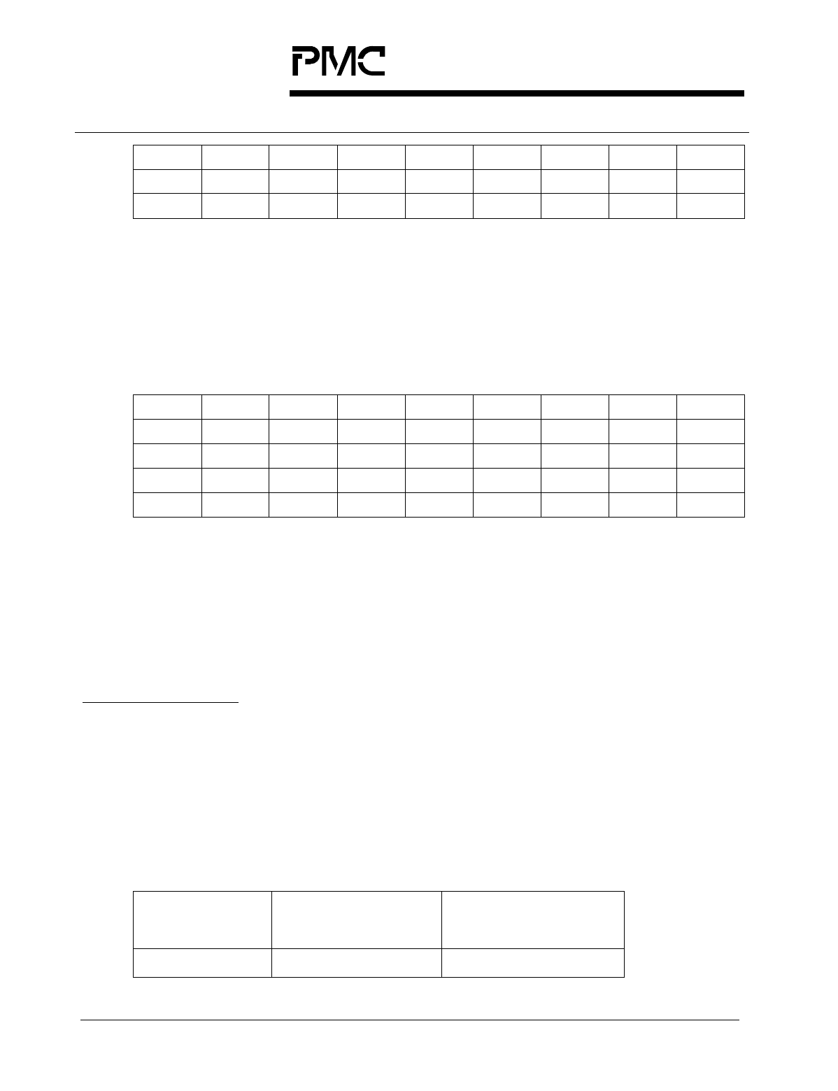
Writing the following address locations forces the outputs to the value in the
corresponding bit position (zeros should be written to all unused test register
locations):
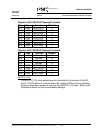
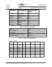
Table 8: Test Mode 0 Write Locations
Addr Bit 7 Bit 6 Bit 5 Bit 4 Bit 3 Bit 2 Bit 1 Bit 0
06H
8BH
8CH
90H
The following outputs can not be controlled using the IOTST feature: D[7:0], and
TDO.
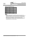
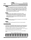
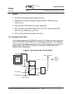
1.
INT corresponds to output INTB. INTB is an open drain output and should be
pulled high for proper operation. Writing a logic one to the INT bit allows the
S/UNI-QUAD to drive INTB low. Writing a logic zero to the INT bit tristates the
INTB output.
12.3
JTAG Test Port
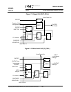
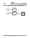
The S/UNI-QUAD JTAG Test Access Port (TAP) allows access to the TAP
controller and the 4 TAP registers: instruction, bypass, device identification and
boundary scan. Using the TAP, device input logic levels can be read, device
outputs can be forced, the device can be identified and the device scan path can
be bypassed. For more details on the JTAG port, please refer to the Operations
section.
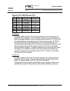
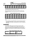
Table 9: Instruction Register (Length - 3 bits)
Instructions Selected Register Instruction Codes,
IR[2:0]
EXTEST Boundary Scan 000


