S/UNI-QUAD
PMC-Sierra, Inc.
PM5349 S/UNI-QUAD
DATASHEET
PMC-971239 ISSUE 6 SATURN USER NETWORK INTERFACE (155-QUAD)
Proprietary and Confidential to PMC-Sierra, Inc., and for its Customers’ Internal Use
61
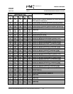
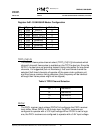
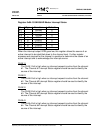
Register 0x01: S/UNI-QUAD Master Configuration
Bit Type Function Default
Bit 7 R/W PECLV 0
Bit 6 R/W Reserved 0
Bit 5 R/W TFPO_CH[1] 0
Bit 4 R/W TFPO_CH[0] 0
Bit 3 R/W Reserved 0
Bit 2 R/W Reserved 0
Bit 1 R/W Reserved 1
Bit 0 R/W Reserved 1
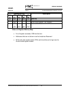
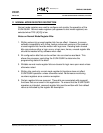
TFPO_CH[1:0]:
The transmit frame pulse channel select (TFPO_CH[1:0]) bits selects which
channel’s transmit frame pulse is available on the TFPO output pin. Since the
RFPO1-4 output pins are providing transmit timing information for loop-timed
channels, it is suggested (but not mandatory) that a self-timed channel be
selected. Self-timed channels all operate off the same clock synthesis unit
and thus have a common timing reference (their frequency will be identical
although their frame pulses might not be aligned).
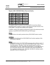
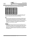
Table 5: TFPO Channel Selection
TFPO_CH[1:0] Selected Channel
00 Channel #1
01 Channel #2
10 Channel #3
11 Channel #4
PECLV:
The PECL reveiver input voltage (PECLV) bit configures the PECL receiver
level shifter. When PECLV is set to logic zero, the PECL receivers are
configured to operate with a 3.3V input voltage. When PECLV is set to logic
one, the PECL receivers are configured to operate with a 5.0V input voltage.


