Chapter 5 Programming Considerations
© National Instruments Corporation 5-7 VXI-MXI User Manual
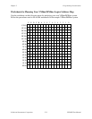
8. Determine the range of addresses that will be occupied by the root device and each first-
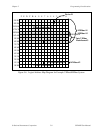
level device and MXIbus link. For Base/Size systems, use the Logical Address Map
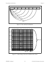
Diagram shown in Figure 5-6 to visualize the logical address map for the system. Each
square in this diagram represents one logical address. The maximum number of logical
addresses in a system is 256 and address ranges are assigned in blocks divisible by a power
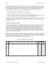
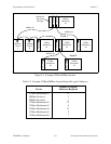
of two. Refer to Table 5-1 and Figure 5-4 for example logical address allocations for
different Size values.
The multiframe RM by definition is located at logical address 0; therefore, the host device of
the multiframe RM must be assigned a range of logical addresses that includes logical
address 0. Starting with the MXIbus link on Level 1, which requires the most logical
addresses, assign the lowest available address range of the logical address map and continue
with the next largest MXIbus link.
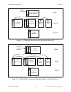
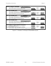
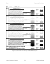
For the example system, VXIbus Mainframe #1, the host to the multiframe RM, requires 16
logical addresses and must have a range that includes logical address 0. It is assigned
address range 0 to F hex. The largest first-level MXIbus link is MXIbus #1. It requires 128
logical addresses, which is one-half of the total logical address space. The lowest available
address range of 128 divisible by a power of two is 80 to FF hex, which is the upper half of
the logical address space. The other first-level MXIbus link, MXIbus #2, only needs eight
logical addresses. It is assigned the lowest available range of size 8: 10 to 17 hex.
9. Determine the range of addresses that will be occupied by each device in the first-level
MXIbus links. Remember that the range of addresses occupied by these devices must be
within the range of addresses assigned to MXIbus link to which it is a member. Start with
the largest device in the MXIbus link.
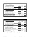
In the example system, MXIbus #1 has four devices. The largest one is VXIbus Mainframe
#3, which requires 64 logical addresses. This device has a second-level MXIbus link that
needs 32 logical addresses, and the mainframe needs eight logical addresses for its own
devices. First, assign the devices in the mainframe to the lowest available range within the
allotted address range of MXIbus #1: 80 to 87 hex. Then assign MXIbus #3 the lowest
available range of size 32: A0 to BF hex. The next largest device, VXIbus Mainframe #2,
needs 32 logical addresses and is assigned the next lowest available range of 32: C0 to DF
hex. MXIbus Device A needs four logical addresses and MXIbus Device B needs one
address. They are assigned E0 to E3, and E4, respectively.
10. Determine the range of addresses that will be occupied by each second-level device and
MXIbus link. Remember that the range of addresses occupied by second-level devices must
be within the range of addresses assigned to the device one level above it. Once the first-
level MXIbus links have been allocated, assign the MXIbus devices and second-level
MXIbus links within the corresponding first-level devices, starting with the largest device.
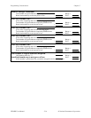
In the example system, we assigned MXIbus #3 address range A0 to BF hex. MXIbus #3
has two devices: VXIbus Mainframe #4 and VXIbus Mainframe #5. Each requires 16
logical addresses; therefore, we assigned them address ranges A0 to AF hex, and B0 to BF
hex, respectively.


