


Chapter 4 Register Descriptions
© National Instruments Corporation 4-41 VXI-MXI User Manual
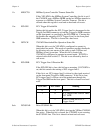
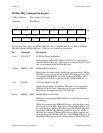
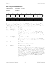
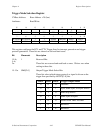
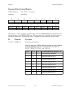
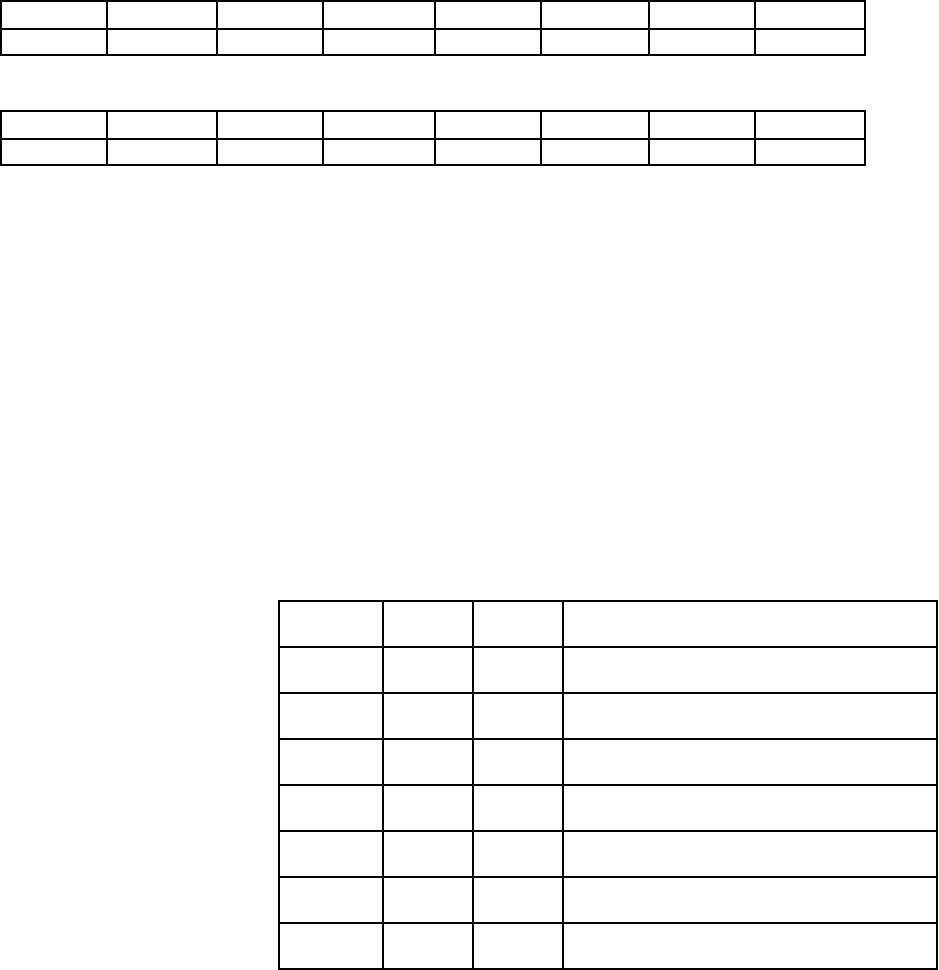
Trigger Mode Selection Register
VXIbus Address: Base Address + 28 (hex)
Attributes: Read/Write
R
15 14 13 12 11 10 9
111
1
11
1
1
8
ITS2 ITS1 ITS0
W
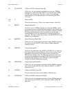
R
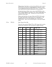
7
654321
1
1
TRIGIN
TRIGOUT ASINT* SSINT*
0
0
ASIE SSIE
W
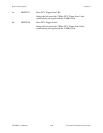
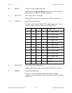
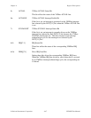
OMS2
OMS1 OMS0 ITS3
ETOE
N
OTS3
OTS2
OTS1
OTS0
ETRI
G
ECLSTAT1
ECLSTAT0
This register configures the ECL and TTL Trigger lines for interrupt generation and trigger
protocol generation. These bits are cleared on soft and hard resets.
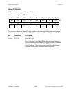
Bit Mnemonic Description
15-8r, 1 Reserved Bits
5-4r,
2w These bits are reserved and read back as ones. Write a zero when
writing to these bits.
15-13w OMS[2-0] Output Trigger Mode Select Bits
These bits select which trigger protocol or signal is driven on the
trigger line specified by the OTS[3-0] bits.
OMS2 OMS1 OMS0 Trigger Output Mode
0 0 0 Disabled
0 0 1 Sync, Semi-Sync, or Async Source
0 1 0 Start-Stop Source
0 1 1 Semi-Sync Acceptor
1 0 0 Source from TRIG IN SMB
1 0 1 Reserved
1 1 X Reserved