Chapter 4 Register Descriptions
© National Instruments Corporation 4-39 VXI-MXI User Manual
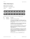
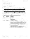
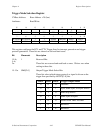
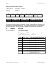
Drive Triggers/Read LA Register
VXIbus Address: Base Address + 26 (hex)
Attributes: Read/Write
R/W
15 14 13 12 11 10 9
DTRIG7 DTRIG6 DTRIG5 DTRIG4
DTRIG3
DTRIG2 DTRIG1 DTRIG0
8
R
7 65432
1
LADD7 LADD6 LADD5 LADD4 LADD3 LADD2 LADD1
LADD0
0
W
00
00
0
PULSE
DRVECL1 DRVECL0
This register provides the logical address of the VXI-MXI and the status of the eight TTL
Trigger lines on the VXIbus. This register is also used to drive the TTL and ECL Trigger lines
individually. The bits in this register are cleared on hard and soft resets.
Bit Mnemonic Description
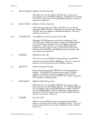
15-8r/w DTRIG[7-0] Drive VXIbus Trigger Lines Bits
Setting these bits asserts the corresponding VXIbus TTL Trigger
line(s) after synchronizing the signal with the 10 MHz clock.
Reading these bits returns the current status of the corresponding
trigger lines.
7-0r LADD[7-0] Logical Address Status Bits
Reading these bits returns the logical address of this VXI-MXI.
The logical address is selected with the DIP switch located at U46.
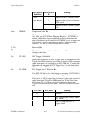
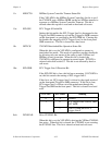
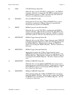
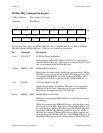
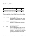
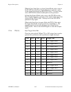
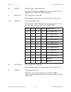
7-3w 0 Reserved Bits
Write a zero when writing to these bits.
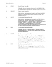
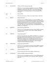
2w PULSE Pulse Selected Trigger Line Bit
Writing a zero to this bit generates either a 100 ns active low pulse
or an active level on the trigger line, as specified by the OTS[2-0]
bits in the Trigger Mode Selection Register. Before another signal
can be generated, a one must be written to this bit. To generate a
stream of pulses, a zero should be written to this bit, immediately
followed by a one. In terms of the START/STOP protocol, writing
a zero to this register generates a START signal on the specified
trigger line and writing a one generates a STOP signal on the
specified trigger line.


