


Chapter 4 Register Descriptions
© National Instruments Corporation 4-31 VXI-MXI User Manual
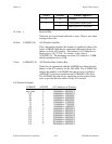
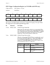
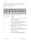
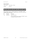
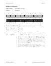
MXIbus Defined Registers
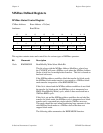
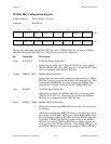
MXIbus Status/Control Register
VXIbus Address: Base Address + 20 (hex)
Attributes: Read/Write
R
15 14 13 12 11 10 9
11MXSCTO INTLCK DSYSFAIL FAIR
8
DSYSFAIL DSYSRST
W
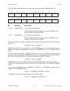
R
7
654321
MXIS
C
LNGMXSCTO MXBER
R
PARERR
0
0
MXTRIGE
N
MXSRSTEN MXACFAILE
N
LNGMXSCTO BOFFCL
R
00
W
RMWMODE
RMWMOD
E
CMODE
CMODE ECL1EN ECL1DIR ECL0EN ECL0DIR
MXTRIGINT MXSRSTINT MXACFAILIN
T
MXSYSFINT
This register contains status and control bits for various types of MXIbus operators.
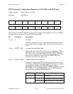
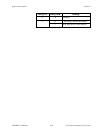
Bit Mnemonic Description
15r/w RMWMODE Read/Modify Write Select Mode Bit
This bit, along with the MXIbus Address Modifiers, selects how
the VXI-MXI will treat a MXIbus cycle when the MXIbus Address
Strobe is held low for multiple data transfers. This bit is cleared on
hard and soft resets.
If the MXIbus address modifiers label the transfer for block mode,
the MXIbus block-mode transfer is converted to a VMEbus block-
mode transfer irrespective of the RMWMODE bit.
If this bit is cleared and the MXIbus address modifiers do not label
the transfer for block mode, the MXIbus cycle is interpreted as a
RMW (Read/Modify/Write) cycle, which is then converted into a
VMEbus RMW cycle.
If this bit is set and the MXIbus address modifiers do not label the
transfer for block mode, the MXIbus cycle is interpreted as a block
transfer and is converted into single transfer VMEbus accesses.
This mode should be used when transferring large amounts of data
with MXIbus block mode to a VMEbus device that does not
support block mode.
The following table summarizes the RMWMODE function.