Chapter 2 General Description
© National Instruments Corporation 2-5 VXI-MXI User Manual
VXI-MXI Functional Description
In simplest terms, the VXI-MXI can be thought of as a bus translator that converts VXIbus
signals into appropriate MXIbus signals. From the perspective of the MXIbus, the VXI-MXI
implements a MXIbus interface to communicate with other MXIbus devices. From the
perspective of the VMEbus, the VXI-MXI is an interface to the outside world.
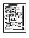
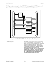
Figure 2-1 is a functional block diagram of the VXI-MXI. Refer to Chapter 6, Theory of
Operation for more details about the major components of the VXI-MXI.
• VMEbus Address and Address Modifiers These transceivers control the direction of the
Transceivers VMEbus address lines and latch the status of the
address lines on the falling edge of the VMEbus
address strobe.
• VXIbus System Controller Functions If the VXI-MXI is selected as the VMEbus
System Controller, this circuitry generates the
16 MHz system clock, provides the VMEbus
arbiter and the VMEbus Bus Timer Unit, and
drives the VXIbus CLK10 signal.
• VMEbus Data Transceivers These transceivers control the direction of the
VMEbus data lines and meet VMEbus
specifications for timing and signal loading.
• VMEbus Control Signals Transceivers These transceivers control the direction of the
VMEbus control signals and meet VMEbus
specifications for timing and signal loading.
• VMEbus Requester and Arbiter Circuitry This circuitry is used to request the VMEbus and
to provide the VMEbus arbiter function if the
VXI-MXI is the VMEbus System Controller.
• TTL and ECL Trigger Lines and This circuitry controls the sending and receiving
CLK10 Circuitry of the TTL and ECL Trigger lines to and from the
SMB connectors on the front panel and from
onboard registers. This logic also controls
whether the VXI-MXI receives the CLK10 signal
from another VXIbus device, or drives the signal
from an onboard 10 MHz oscillator or from an
external signal connected to the EXT CLK SMB
connector on the front panel.
• SYSFAIL, ACFAIL, and SYSRESET Through this circuitry, the VMEbus signals
SYSFAIL, ACFAIL and SYSRESET connect to
the corresponding signals on the daughter card
connections. These three signals can also be
individually enabled to generate a VMEbus
interrupt. With control bits in onboard registers,
SYSFAIL and SYSRESET can also be driven on
the VMEbus backplane.


