Register Descriptions Chapter 4
VXI-MXI User Manual 4-10 © National Instruments Corporation
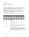
Logical Address Window Register
VXIbus Address: Base Address + A (hex)
Attributes: Read/Write
This register defines the range of logical addresses that are mapped into and out of the VXI-MXI
through the MXIbus. This register defines a configuration window in the upper 16 KB of A16
space. These bits are cleared on a hard reset.
The CMODE bit in the MXIbus Control Register selects the format of this register. If the
CMODE bit is 0 (default), a Base/Size window comparison is used to determine the range of
addresses in the window. If the CMODE bit is set, an upper and lower bound is used to
determine the range of addresses in the window.
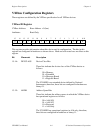
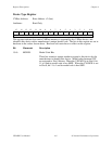
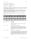
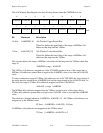
The Logical Address Window Register has the following format when the CMODE bit is
cleared:
R/W
7 65432
1
LABASE7 LABASE6 LABASE5 LABASE4 LABASE3 LABASE2
LABASE1
LABASE0
0
R
15 14 13 12 11 10 9
0 LAEN LADIR 1 1 LASIZE2 LASIZE1
LASIZE0
8
0
LAEN
LADIR 0 0 LASIZE2 LASIZE1 LASIZE0
W
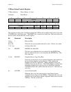
Bit Mnemonic Description
15r/w 0 Reserved Bit
This bit is reserved and reads back as zero. Write a zero when
writing to these bits.
14r/w LAEN Logical Address Window Enable Bit
When this bit is set, the logical address mapping window is
enabled. When this bit is cleared, the logical address mapping
window is disabled except for the logical address of this device.
Access to the VXI-MXI's own configuration space is always
enabled.
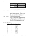
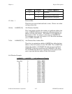
13r/w LADIR Logical Address Window Direction Bit
When this bit is set, the logical address window applies to MXIbus
cycles that are mapped into VXIbus cycles (inward cycles). When
this bit is cleared, the logical address window applies to VXIbus
cycles that are mapped out into MXIbus cycles (outward cycles).
The complement of the defined range is mapped in the opposite
direction.


