Configuration and Installation Chapter 3
VXI-MXI User Manual 3-6 © National Instruments Corporation
VXIbus Logical Address
Each device in a VXIbus/MXIbus system is assigned a unique number between 0 and 254. This
8-bit number, called the logical address, defines the base address for the configuration registers
located on the device. With unique logical addresses, each VXIbus device in the system is
assigned 64 bytes of configuration space in the upper 16 KB of A16 space.
Some VXIbus devices have dynamically configurable logical addresses. These devices have an
initial logical address of hex FF, which indicates that they can be dynamically configured. While
the VXI-MXI does support dynamic configuration of VXIbus devices within its mainframe, it
cannot itself be dynamically configured. Therefore, do not set the logical address for the
VXI-MXI to hex FF.
The VXIbus RM has Logical Address 0 by definition. The VXI-MXI does not have VXIbus RM
capability, so do not set the logical address for the VXI-MXI to 0. If you are configuring a
multiple-mainframe VXIbus/MXIbus system, refer to Chapter 5, Programming Considerations,
for instructions on planning a VXIbus/MXIbus system logical address map. If you are
connecting only a PC with a MXIbus interface to the VXI-MXI, you should leave the logical
address at the default setting of 1. Using this setting, you can install devices with all other
possible logical addresses in the VXIbus mainframe.
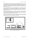
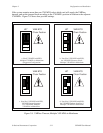
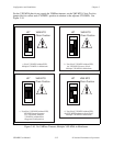
An 8-bit DIP switch selects the logical address for the VXI-MXI. As shown in Figure 3-1, this
switch is labeled LOGICAL ADDRESS SWITCH on the front panel. The ON position on the DIP
switch corresponds to a logic value of 0, and the OFF position corresponds to a logic value of 1.
This switch is set at the factory to a default logical address of 1. Verify that the logical address
assigned to the VXI-MXI is not used by any other statically configured VXIbus device in your
system. Remember that logical addresses hex 0 and FF are not allowed for the VXI-MXI.
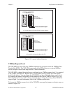
Figure 3-5 shows switch settings for logical address hex 1 and C0.


