Chapter 6 Theory of Operation
© National Instruments Corporation 6-11 VXI-MXI User Manual
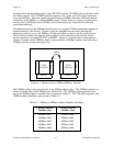
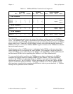
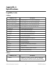
Table 6-3. When a transfer involving an address in one of the inward windows is detected, the
VXI-MXI begins arbitrating for the VMEbus. When the VXI-MXI wins the VMEbus, the
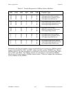
MXIbus transfer is converted into a VMEbus transfer. The data transfer size information is
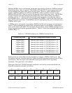
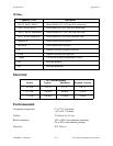
converted from MXIbus signals to VMEbus signals as shown in Table 6-4. The transfer is
complete when the responding VMEbus device sends a DTACK or BERR signal across the
MXIbus and the remote MXIbus device releases the address strobe and data strobe.
The VXI-MXI circuitry generates and checks parity during the address and data portions of all
MXIbus cycles. The VMEbus is not requested if the MXIbus address received has a parity error.
Parity is also checked when MXIbus data is written to the VXI-MXI slave circuitry. If a parity
error occurs, the bad data is not written to the VMEbus and a BERR is sent back to the MXIbus
master. The MXIbus PAR* signal is generated and sent during a MXIbus slave read cycle.
When the MXIbus address strobe remains low during multiple data transfers, the VXI-MXI
interprets the transfer in one of three ways, depending upon the information sent on the address
modifier lines and the state of the RMWMODE bit in the MXIbus Status/Control Register:
1. If the address modifiers indicate a MXIbus block-mode transfer, the MXIbus transfer is
converted directly into a VMEbus block-mode transfer, regardless of the state of the
RMWMODE bit. MXIbus does not limit the length of the block transfer in any way;
however, the VMEbus specification limits VMEbus block transfers to a maximum of 256
bytes in length. The VXI-MXI, therefore, will initiate a new block transfer after every 256
bytes of the MXIbus block transfer.
2. If the RMWMODE bit is 0 and the address modifiers sent across the MXIbus indicate a non-
VMEbus block-mode transfer, the MXIbus transfer is interpreted as a read/modify/write
(RMW) cycle and is converted into a VMEbus RMW cycle.
3. If the RMWMODE bit is 1 and the address modifiers sent across the MXIbus indicate a non-
VMEbus block-mode transfer, the VXI-MXI uses onboard 32-bit counters to convert the
MXIbus block-mode transfer into many VMEbus single cycle transfers. All MXIbus slaves
are required to latch the MXIbus address into onboard address counters on the assertion edge
of AS* and increment the counters on each trailing edge of DS*.
The length of a MXIbus block transfer is not limited to the address space of a single MXIbus
device. A MXIbus master can perform a single block-mode transfer to multiple address-
consutive MXIbus slaves. For this reason, each MXIbus slave must continually monitor the
address count of all MXIbus block-mode transfers and decode the output of the address counters
to determine if the block transfer crosses into its inward address window. At any time the
transfer can cross into one of the VXI-MXI's inward windows, requiring the circuitry to respond
to the transfer.
MXIbus Address/Data and Address Modifier Transceivers
The MXIbus address/data transceivers and the associated circuitry multiplex and de-multiplex
the MXIbus address and data information from the MXIbus AD[31-0] lines and control the
direction of address and data flow. Address and address modifier information from the MXIbus
is latched on the rising edge of the MXIbus address strobe. The address is latched into address
counters that are incremented on each falling edge of the MXIbus data strobe.


