Register Descriptions Chapter 4
VXI-MXI User Manual 4-28 © National Instruments Corporation
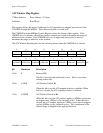
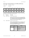
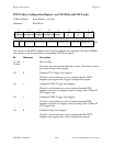
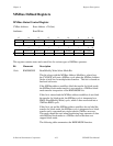
INTX Utility Configuration Register (on VXI-MXIs with INTX only)
VXIbus Address: Base Address + 18 (hex)
Attributes: Read/Write
R
15 14 13 12 11 10 9
0 1 101 111
8
R/W
7654321
1 1 ACFAILIN ACFAILOUT SYSFAILIN SYSFAILOUT SYSRSTIN SYSRSTOUT
0
0 0 000 000
W
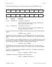
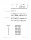
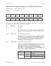
This register on the INTX daughter card is used to configure the mapping of the three VMEbus
reset signals to and from the three corresponding INTX reset signals.
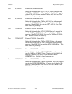
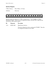
Bit Mnemonic Description
15-12w, 1 Reserved Bits
11-6r/w
These bits are reserved and read back as ones. Write zeros to these
bits when writing to this register.
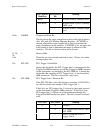
15r 0 Extended TTL Trigger Line Support
This bit is set in hardware to zero to indicate that the INTX
daughter card supports the Trigger Configuration register.
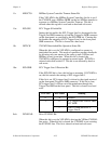
14r 1 Extended P3 ECL Trigger Line Support
This bit is set in hardware to one to indicate that the INTX
daughter card does not support external routing of the VXIbus P3
ECL trigger lines.
13r 1 Extended P2 ECL Trigger Line Support
This bit is set in hardware to one to indicate that the INTX
daughter card does not support external routing of the VXIbus P2
ECL trigger lines.
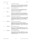
12r 0 Extended Utility Line Support
This bit is set in hardware to zero to indicate that the INTX
daughter card supports this Utility Configuration register.


